Hitachi HD74ALVCH16830
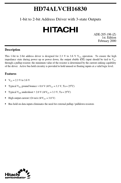
This 1-bit to 2-bit address driver is designed for 2.3 V to 3.6 V V CC operation. These are stress ratings only, and functional operation of the device at these or any other conditions beyond those indicated under “recommended operating conditions” is not implied.| Part No. | HD74ALVCH16830 |
|---|---|
| Datasheet | HD74ALVCH16830 Download |
| Manufacturer |  Hitachi |
| Description | 1-bit to 2-bit Address Driver with 3-state Outputs |
| Buy | Stock & Price |
DESCRIPTION
To ensure the high impedance state during power up or power down, the output ebable (OE ) input should be tied to VCC through a pullup resistor; the minimum value of the resistor is determined by the current sinking capability of the driver. Active bus hold circuitry is provided to hold unused or floating inputs at a valid logic level.FEATURES
● VCC = 2.3 V to 3.6 V● Typical VOL ground bounce < 0.8 V (@VCC = 3.3 V, Ta = 25°C)
● Typical VOH undershoot > 2.0 V (@VCC = 3.3 V, Ta = 25°C)
● High output current ±24 mA (@V CC = 3.0 V)
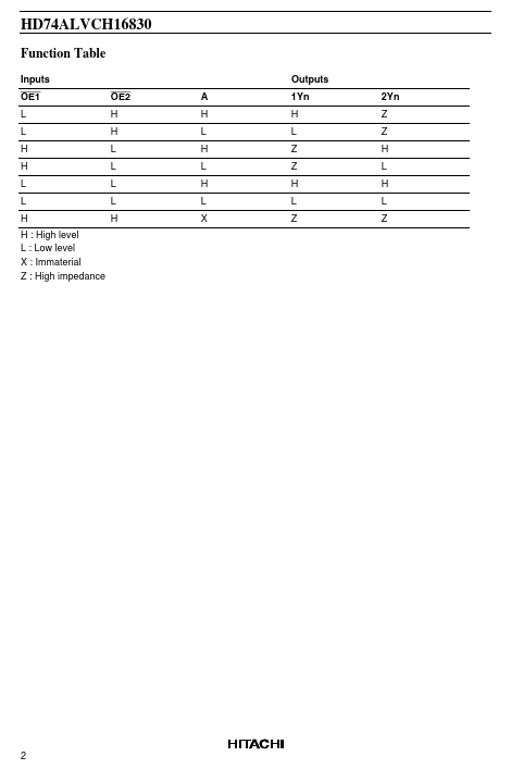
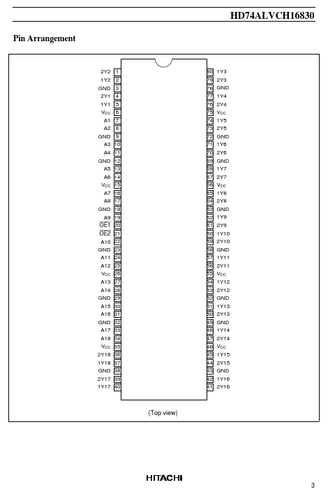
● Bus hold on data inputs eliminates the need for external pullup / pulldown resistors HD74ALVCH16830 Function Table Inputs OE1 L L H H L L H H : High level L : Low level X : Immaterial Z : High impedance OE2 H H L L L L H A H L H L H L X Outputs 1Yn H L Z Z H L Z 2Yn Z Z H L H L Z 2 HD74ALVCH16830 Pin Arrangement 2Y2 1Y2 GND 2Y1 1Y1 VCC A1 A2 GND A3 A4 GND A5 A6 VCC A7 A8 GND A9 OE1 OE2 A10 GND A11 A12 VCC A13 A14 GND A15 A16 GND A17 A18 VCC 2Y18...