2SK1934
2SK1934 is Silicon N-Channel MOSFET manufactured by Hitachi Semiconductor.
Features
- -
- - Low on- resistance High speed switching No secondary breakdown Suitable for Switching regulator
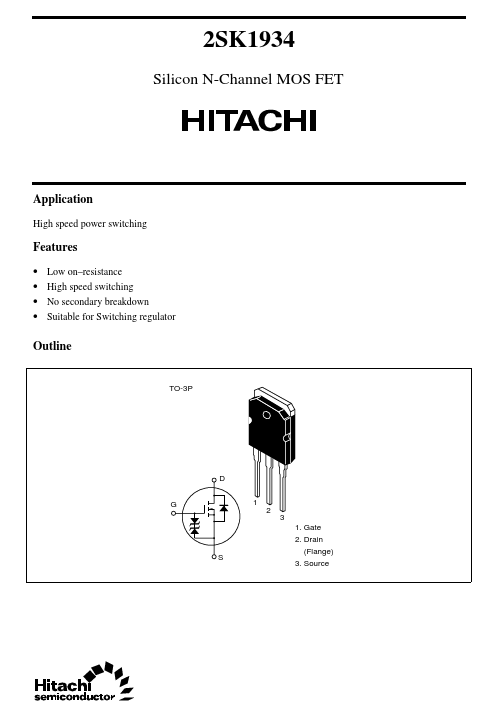
Outline
TO-3P
D G 1 2 3 1. Gate 2. Drain (Flange) 3. Source
Absolute Maximum Ratings (Ta = 25°C)
Item Drain to source voltage Gate to source voltage Drain current Drain peak current Body to drain diode reverse drain current Channel dissipation Channel temperature Storage temperature Notes 1. PW ≤ 10 µs, duty cycle ≤ 1 % 2. Value at Tc = 25°C Symbol VDSS VGSS ID I D(pulse)- I DR Pch- Tch Tstg
2 1
Ratings 1000 ±30 8 24 8 150 150
- 55 to +150
Unit V V A A A W °C °C
Electrical Characteristics (Ta = 25°C)
Item Drain to source breakdown voltage Gate to source breakdown voltage Gate to source leak current Symbol V(BR)DSS V(BR)GSS I GSS Min 1000 ±30
- - 2.0
- 4
- -
- -
- -
- -
- Typ
- -
- -
- 1.2 6 2690 920 375 35 135 300 205 0.9 1600 Max
- - ±10 250 3.0 1.6
- -
- -
- -
- -
- - Unit V V µA µA V Ω S p F p F p F ns ns ns ns V µs I F = 8 A, VGS = 0 I F = 8 A, VGS = 0, di F / dt = 100 A / µs Test conditions I D = 10 m A, VGS = 0 I G = ±100 µA, VDS = 0 VGS = ±25 V, VDS = 0 VDS = 800 V, VGS = 0 I D = 1 m A, VDS = 10 V ID = 4 A VGS = 10 V- 1 ID = 4 A VDS = 20 V- 1 VDS = 10 V VGS = 0 f = 1 MHz ID = 4 A VGS = 10 V RL = 7.5 Ω
Zero gate voltage drain current I DSS Gate to source cutoff voltage Static drain to source on state resistance Forward transfer admittance Input capacitance Output capacitance Reverse transfer capacitance Turn-on delay time Rise time Turn-off delay time Fall time Body to drain diode forward voltage Body to drain diode reverse recovery time Note 1. Pulse Test VGS(off) RDS(on) |yfs| Ciss Coss Crss t d(on) tr t d(off) tf VDF t rr
Power vs. Temperature Derating 150 Channel Dissipation Pch (W) Drain Current I D (A) Maximum Safe Operation Area ar ea )
50 30 10 3 1 0.3 0.1
10 µs µs s 0 10 1 m
O is pe lim ra ite tion d in by t R his D
S( on
100 m c= (T 10 n = tio ra pe O
DC s (1 sh...