2SK2216
2SK2216 is Silicon N-Channel MOS FET manufactured by Hitachi Semiconductor.
Features
- High power output, high gain, high efficiency PG = 9.7 d B, Pout = 140 W, ηD = 55% typ (f = 860 MHz)
- pact package Suitable for push
- pull circuit
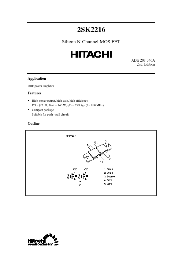
Outline
Absolute Maximum Ratings (Ta = 25°C)
Item Drain to source voltage Gate to source voltage Drain current Channel dissipation Channel temperature Storage temperature Note: 1. Value at TC = 25°C Symbol VDSS VGSS ID Pch- Tch Tstg
Ratings 60 ±10 20 150 150
- 55 to +150
Unit V V A W °C °C
Electrical Characteristics (TC = 25°C)
Item Drain leakage current-
1 1 1
Symbol Min I DSS I GSS VGS(off) VDS(on) |yfs| Ciss Coss POUT ηD
Typ
- -
- 1.2 4.0 250 85 140 55
Max 1 ±3 1.6 2.5
- -
- -
- Unit m A µA V V S p F p F W %
Test conditions VDS = 60 V, VGS = 0 VGS = ± 10 V, VDS = 0 VDS = 10 V, ID = 1 m A VGS = 10 V, ID = 5 A- 2 VDS = 10 V, ID = 5 A- 2 VGS = 5 V, VDS = 0 f = 1MHz VDS = 10V, VGS = 0 f = 1MHz VDS = 28 V, IDO = 0.4 A f = 860 MHz, Pin = 15 W
- - 0.3
- 3.0
- - 100
- Gate leakage current-
Gate to source cutoff voltage- Drain to source voltage-
Forward transfer admittance- 1 Input capacitance- 1 Output capacitance- 1 Output power Drain efficiency Notes: 1. Shows / unit FET 2. Pulse Test
Package Dimensions
Unit: mm
When using this document, keep the following in mind: 1. This document may, wholly or partially, be subject to change without notice. 2. All rights are reserved: No one is permitted to reproduce or duplicate, in any form, the whole or part of this document without Hitachi’s permission. 3. Hitachi will not be held responsible for any damage to the user that may result from accidents or any other reasons during operation of the user’s unit according to this document. 4. Circuitry and other examples described herein are meant merely to indicate the characteristics and performance of Hitachi’s semiconductor products. Hitachi assumes no responsibility for any intellectual property claims or other problems that may result...