2SK2373
2SK2373 is N-Channel MOSFET manufactured by Hitachi Semiconductor.
Features
- -
- -
- Low on-resistance Small package Low drive current 4 V gate drive device can be driven from 5 V source. Suitable for low signal load switch
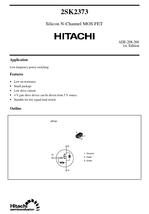
Outline
MPAK
3 1 2 D 1. Source 2. Gate 3. Drain
Absolute Maximum Ratings (Ta = 25°C)
Item Drain to source voltage Gate to source voltage Drain current Drain peak current Body to drain diode reverse drain current Channel dissipation Channel temperature Storage temperature Notes 1. PW ≤ 100 µs, duty cycle ≤ 10 % 2. Marking is “ZE- ”. Symbol VDSS VGSS ID I D(pulse)- I DR Pch- Tch Tstg
2 1
Ratings 30 ±20 0.2 0.4 0.2 150 150
- 55 to +150
Unit V V A A A m W °C °C
Electrical Characteristics (Ta = 25°C)
Item Drain to source breakdown voltage Gate to source breakdown voltage Gate to source leak current Symbol V(BR)DSS V(BR)GSS I GSS Min 30 ±20
- - 1.0
- - Input capacitance Output capacitance Reverse transfer capacitance Turn-on delay time Rise time Turn-off delay time Fall time Note 1. Pulse Test Ciss Coss Crss t d(on) tr t d(off) tf
- -
- -
- -
- Typ
- -
- -
- 1.4 1.0 17.8 25.4 3.7 50 125 660 400 Max
- - ±2 1 2.0 2.5 1.4
- -
- -
- -
- Unit V V µA µA V Ω Ω p F p F p F ns ns ns ns Test Conditions I D = 100 µA, VGS = 0 I G = ±100 µA, VDS = 0 VGS = ±16 V, VDS = 0 VDS = 30 V, VGS = 0 I D = 10 µA, VDS = 5 V I D = 20 m A VGS = 4 V- 1 I D = 10 m A VGS = 10 V- 1 VDS = 10 V VGS = 0 f = 1 MHz I D = 0.1 A VGS = 10 V RL = 100 Ω PW = 2 µs
Zero gate voltage drain current I DSS Gate to source cutoff voltage Static drain to source on state resistance VGS(off) RDS(on)
Pch (m W) Maximum Channel Dissipation Curve 200 I D (A)
Maximum Safe Operation Area 1 ms
0.3 0.1
= s PW0 m 1
Channel Power Dissipation
Drain Current n tio ra pe O
0.03 0.01 0.003...