6AM14
6AM14 is Silicon N-Channel/P-Channel Power MOS FET Array manufactured by Hitachi Semiconductor.
Features
- -
- - Low on-resistance Low drive current High speed switching High density mounting
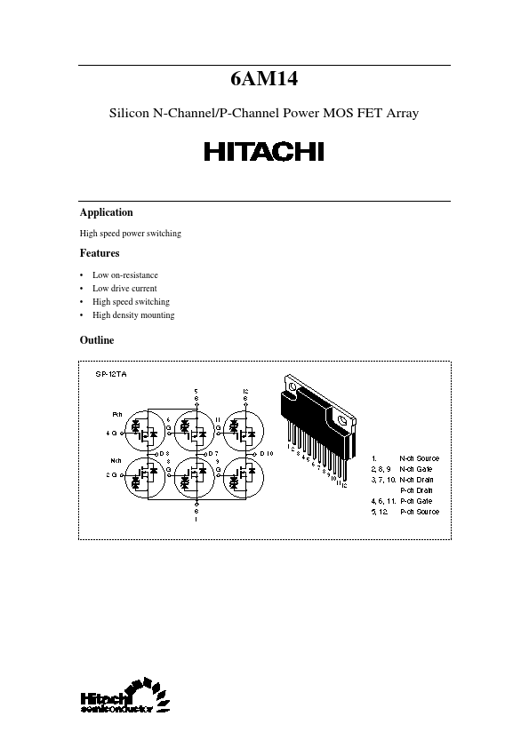
Outline
Absolute Maximum Ratings (Ta = 25°C)
Ratings Item Drain to source voltage Gate to source voltage Drain current Drain peak current Reverse drain current Channel dissipation Channel dissipation Channel temperature Storage temperature Notes: 1. PW ≤ 10 µs, duty cycle ≤ 1% 2. Value at 6 Drive operation Symbol VDSS VGSS ID ID(pulse)- 1 IDR Pch- 2 Pch- 2 Tch Tstg Nch 60 ±20 7 28 7 42 4.8 150
- 55 to +150 Pch
- 60 ±20
- 7
- 28
- 7 Unit V V A A A W W °C °C
Electrical Characteristics N Channel (Ta = 25°C)
Item Drain to source breakdown voltage Gate to source breakdown voltage Gate to source leak current Symbol Min Typ
- -
- -
- 0.14 Max
- - ±10 250 1.5 0.2 Unit V V µA µA V Ω Test conditions ID = 10 m A, VGS = 0 IG = ±100 µA, VDS = 0 VGS = ±16 V, VDS = 0 VDS = 50 V, VGS = 0 VDS = 10 V, ID = 1 m A ID = 4 A VGS = 4 V- 1
- 0.22 0.5 Ω ID = 2 A VGS = 2.5 V- 1 Forward transfer admittance |yfs| 4.0 6.5
- S ID = 4 A VDS = 10 V- 1 Input capacitance Output capacitance Reverse transfer capacitance Turn-on delay time Rise time Turn-off delay time Fall time Body to drain diode forward voltage Body to drain diode reverse recovery time Note: 1. Pulse Test Ciss Coss Crss td(on) tr td(off) tf VDF trr
- -
- -
- -
- -
- 500 240 30 15 90 110 250 1.0 170
- -
- -
- -
- -
- p F p F p F ns ns ns ns V ns IF = 7 A, VGS = 0 IF = 7 A, VGS = 0 di F/dt = 50 A/µs VDS = 10 V VGS = 0 f = 1 MHz VGS = 10 V, ID = 4 A RL = 7.5 Ω
V(BR)DS 60 S V(BR)GS ±20 S IGSS
- -
Zero gate voltage drain current IDSS Gate to source cutoff voltage Static drain to source on state resistance
VGS(off) 0.5 RDS(on)
- 3
Electrical Characteristics P Channel (Ta = 25°C)
Item Drain to source breakdown voltage Gate to source breakdown voltage Gate to source leak current Symbol Min Typ
- -
- -
- 0.12 Max
- -...