HY27SSxxx
description of Device Operations
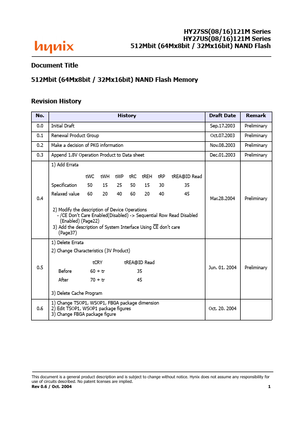
- /CE Don’t Care Enabled(Disabled) -> Sequential Row Read Disabled (Enabled) (Page22) 3) Add the description of System Interface Using CE don’t care (Page37) 1) Delete Errata 2) Change Characteristics (3V Product) 0.5 t CRY Before After 60 + tr 70 + tr t REA@ID Read 35 45 Jun. 01. 2004 Preliminary
3) Delete Cache Program 0.6 1) Change TSOP1, WSOP1, FBGA package dimension 2) Edit TSOP1, WSOP1 package figures 3) Change FBGA package figure Oct. 20. 2004
This document is a general product description and is subject to change without notice. Hynix does not assume any responsibility for use of circuits described. No patent licenses are implied. Rev 0.6 / Oct. 2004 1
HY27SS(08/16)121M Series HY27US(08/16)121M Series 512Mbit (64Mx8bit / 32Mx16bit) NAND Flash FEATURES
SUMMARY
HIGH DENSITY NAND FLASH MEMORIES
- Cost effective solutions for mass storage applications
FAST BLOCK ERASE
- Block erase time: 2ms (Typ)
NAND INTERFACE
- x8 or x16 bus width.
-...