HY27UH088GDM
features
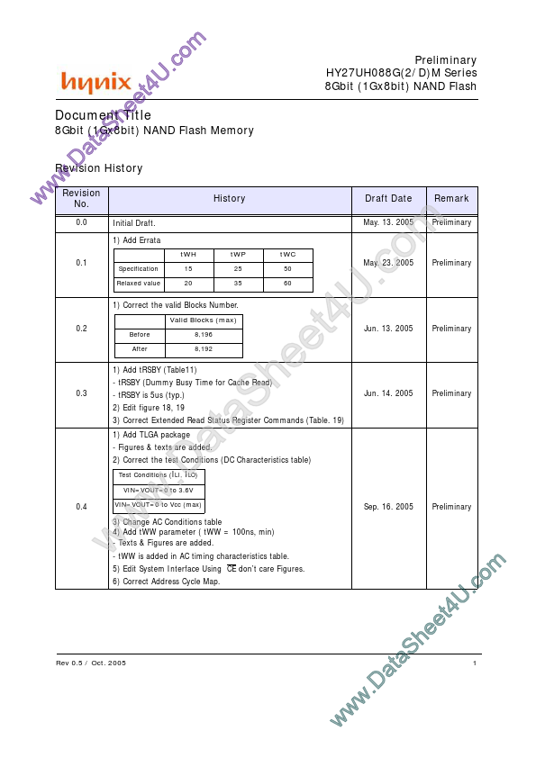
. 9) Change AC Characteristics
- Errata is deleted. t WC Before After 0.4
- t R is change t R Before After 25us 30us 60ns 50ns t WP 35ns 25ns t WH 20ns 15ns Sep. 16. 2005 Preliminary
10) Change DC Characteristics (Table 8)
- Operation Current ICC1 Typ Before After 30 40 ICC2 Typ 30 40 ICC3 Typ 30 40 ILI Max ILO Max
± 20 ± 20 ± 40 ± 40
1) Delete Concurrent Operation.
Oct. 05. 2005
Preliminary
Rev 0.5 / Oct. 2005
Preliminary HY27UH088G(2/D)M Series 8Gbit (1Gx8bit) NAND Flash FEATURES
SUMMARY
HIGH DENSITY NAND FLASH MEMORIES
- Cost effective solutions for mass storage applications NAND INTERFACE
- x8 bus width.
- Multiplexed Address/ Data
- Pinout patibility for all densities STATUS REGISTER ELECTRONIC SIGNATURE
- Manufacturer Code
- Device Code CHIP ENABLE DON'T CARE OPTION
- Simple interface with microcontroller AUTOMATIC PAGE 0 READ AT POWER-UP OPTION
- Boot from NAND support
- Automatic Memory Download SERIAL NUMBER OPTION HARDWARE DATA PROTECTION PAGE SIZE
- x8...