Datasheet4U Logo Datasheet4U.com

HY27US16281A - (HY27USxx281A) 128Mbit (16Mx8bit / 8Mx16bit) NAND Flash Memory

Download the HY27US16281A datasheet PDF. This datasheet also covers the HY27US08281A variant, as both devices belong to the same (hy27usxx281a) 128mbit (16mx8bit / 8mx16bit) nand flash memory family and are provided as variant models within a single manufacturer datasheet.

General Description

& page.7 - The Cache feature is deleted in summary description.

- Note.3 is deleted.

Key Features

  • 2) Change AC Conditions table 3) Add tWW parameter ( tWW = 100ns, min) - Texts & Figures are added. - tWW is added in AC timing characteristics table. 4) Edit Copy Back Program operation step 5) Edit System Interface Using CE don’t care Figures. 6) Correct Address Cycle Map. 1) Correct PKG dimension (TSOP, USOP PKG) CP 0.5 Before After 0.6 0.050 0.100 Nov. 07. 2005 Sep. 02. 2005 0.4 Jul. 26. 2005 1) Correct USOP figure. Rev 0.6 / Nov. 2005 2 HY27US(08/16)281A Series 128Mbit (16Mx8bit / 8M.

📥 Download Datasheet

Note: The manufacturer provides a single datasheet file (HY27US08281A_HynixSemiconductor.pdf) that lists specifications for multiple related part numbers.

Datasheet Details

Part number HY27US16281A
Manufacturer SK Hynix
File Size 412.36 KB
Description (HY27USxx281A) 128Mbit (16Mx8bit / 8Mx16bit) NAND Flash Memory
Datasheet download datasheet HY27US16281A Datasheet

Full PDF Text Transcription for HY27US16281A (Reference)

Note: Below is a high-fidelity text extraction (approx. 800 characters) for HY27US16281A. For precise diagrams, and layout, please refer to the original PDF.

HY27US(08/16)281A Series 128Mbit (16Mx8bit / 8Mx16bit) NAND Flash Document Title 128Mbit (16Mx8bit / 8Mx16bit) NAND Flash Memory Revision History
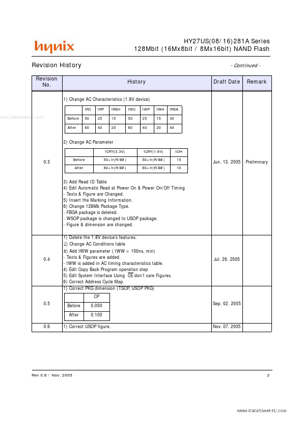
 Revision No. www.DataShe...

View more extracted text
8Mx16bit) NAND Flash Memory Revision History Revision No. www.DataSheet4U.com 0.0 Initial Draft. 1) Correct Summary description & page.7 - The Cache feature is deleted in summary description. - Note.3 is deleted. (page.7) 2) Correct table.5 & Table.12 3) Correct TSOp1, WSOP1 Pin description - 38th pin has been changed Lockpre 4) Add Bad Block Management & System Interface using CE don’t care 5) Change TSOP1, WSOP1, FBGA package dimension & figures. - Change TSOP1, WSOP1, FBGA package mechanical data - Change TSOP1, WSOP1 package figures 1) LOCKPRE is changed to PRE. - Texts, Tables and figures are changed. 2) Change Comma