Datasheet4U Logo Datasheet4U.com

HY57V641620ET - 4-Bank x 1M x 16-Bits SDRAM

General Description

and is subject to change without notice.

Hynix does not assume any responsibility for use of circuits described.

No patent licenses are implied.

Key Features

  • Voltage: VDD, VDDQ 3.3V supply voltage All device pins are compatible with LVTTL interface 54 Pin TSOPII (Lead or Lead Free Package) All inputs and outputs referenced to positive edge of system clock Data mask function by UDQM, LDQM.
  • Internal four banks operation.
  • Burst Read Single Write operation Programmable CAS Latency; 2, 3 Clocks.
  • Auto refresh and self refresh 4096 Refresh cycles / 64m.

📥 Download Datasheet

Full PDF Text Transcription (Reference)

The following content is an automatically extracted verbatim text from the original manufacturer datasheet and is provided for reference purposes only.

View original datasheet text
m o c . 64Mb Synchronous DRAM based on 1M x 4Bank x16 I/O U 4 t e e Document Title h S a Revision at History .D w w w 
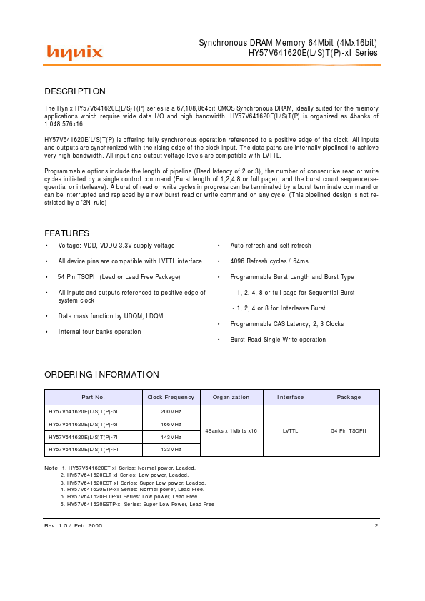
4Bank x 1M x 16bits Synchronous DRAM 
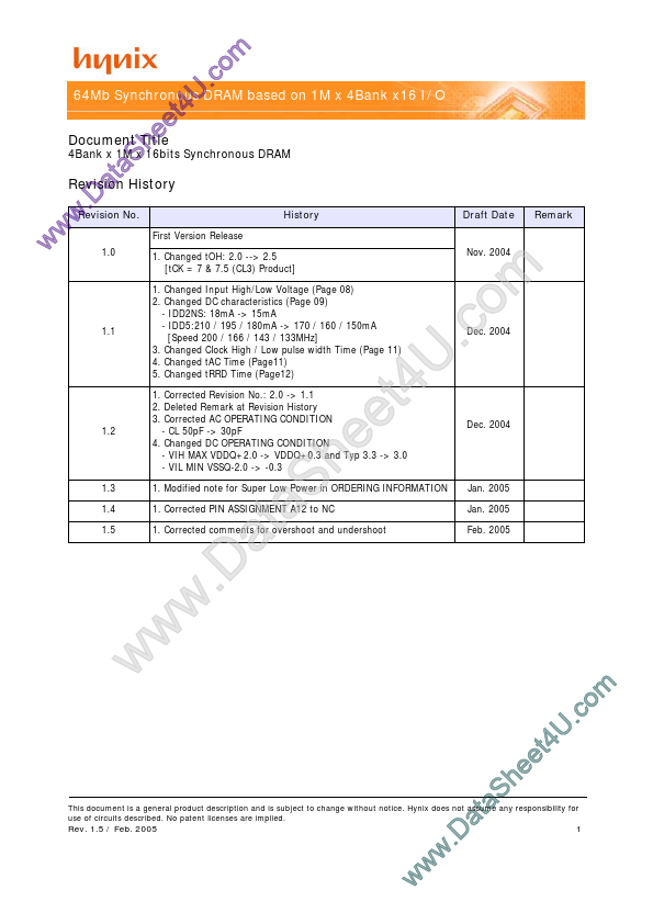
Revision No. History First Version Release 1.0 1. Changed tOH: 2.0 --> 2.5 [tCK = 7 & 7.5 (CL3) Product] 1.1 1. Changed Input High/Low Voltage (Page 08) 2. Changed DC characteristics (Page 09) - IDD2NS: 18mA -> 15mA - IDD5:210 / 195 / 180mA -> 170 / 160 / 150mA [Speed 200 / 166 / 143 / 133MHz] 3. Changed Clock High / Low pulse width Time (Page 11) 4. Changed tAC Time (Page11) 5. Changed tRRD Time (Page12) Draft Date Remark Nov. 2004 1.2 1.3 1.4 1.5 m o .c U 4 t e e h S a t a .D w w w Dec. 2004 1. Corrected Revision No.: 2.0 -> 1.1 2. Deleted Remark at Revision History 3. Corrected AC OPERATING CONDITION - CL 50pF -> 30pF 4.