Datasheet4U Logo Datasheet4U.com

HY57V641620FTP - Synchronous DRAM Memory 64Mbit

General Description

and is subject to change without notice.

Hynix does not assume any responsibility for use of circuits described.

No patent licenses are implied.

Key Features

  • Voltage: VDD, VDDQ 3.3V supply voltage All device pins are compatible with LVTTL interface 54 Pin TSOPII (Lead or Lead Free Package) All inputs and outputs referenced to positive edge of system clock Data mask function by UDQM, LDQM.
  • Internal four banks operation.
  • Burst Read Single Write operation Programmable CAS Latency; 2, 3 Clocks.
  • Auto refresh and self refresh 4096 Refresh cycles / 64m.

📥 Download Datasheet

Full PDF Text Transcription (Reference)

The following content is an automatically extracted verbatim text from the original manufacturer datasheet and is provided for reference purposes only.

View original datasheet text
64Mb Synchronous DRAM based on 1M x 4Bank x16 I/O Document Title 4Bank x 1M x 16bits Synchronous DRAM Revision History Revision No. 0.1 History Initial Draft Draft Date Jan. 2007 Remark Preliminary This document is a general product description and is subject to change without notice. Hynix does not assume any responsibility for use of circuits described. No patent licenses are implied. Rev. 0.1 / Jan. 2007 1 Free Datasheet http://www.0PDF.com 
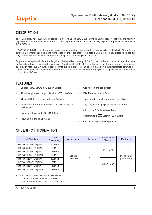
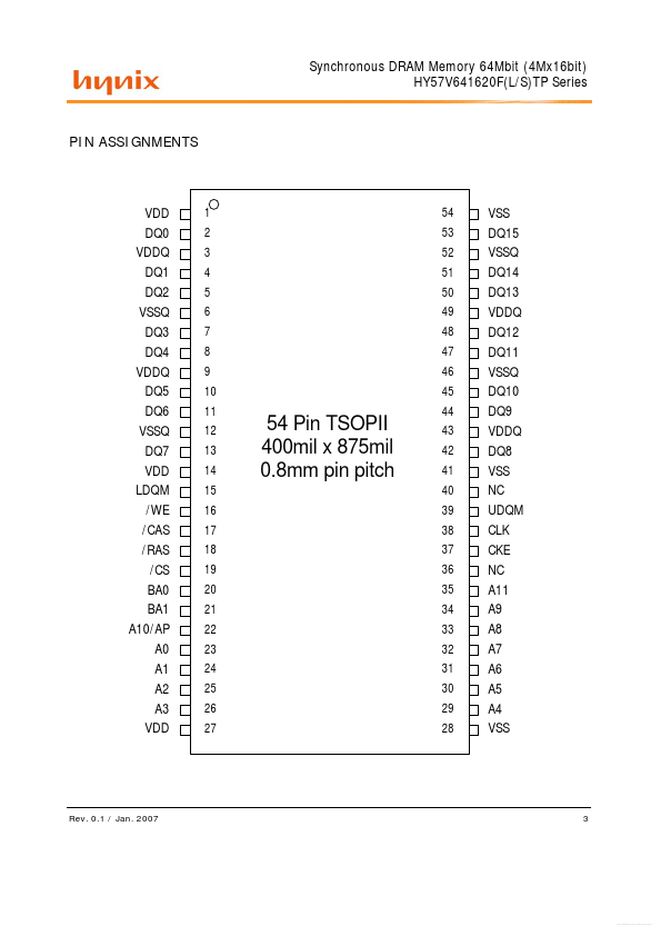
Synchronous DRAM Memory 64Mbit (4Mx16bit) HY57V641620F(L/S)TP Series DESCRIPTION The Hynix HY57V641620F(L/S)TP series is a 67,108,864bit CMOS Synchronous DRAM, ideally suited for the memory applications which require wide data I/O and high bandwidth. HY57V641620F(L/S)TP is organized as 4banks of 1,048,576x16.