HY62UF16804A
HY62UF16804A is 512Kx16bit full CMOS SRAM manufactured by SK Hynix.
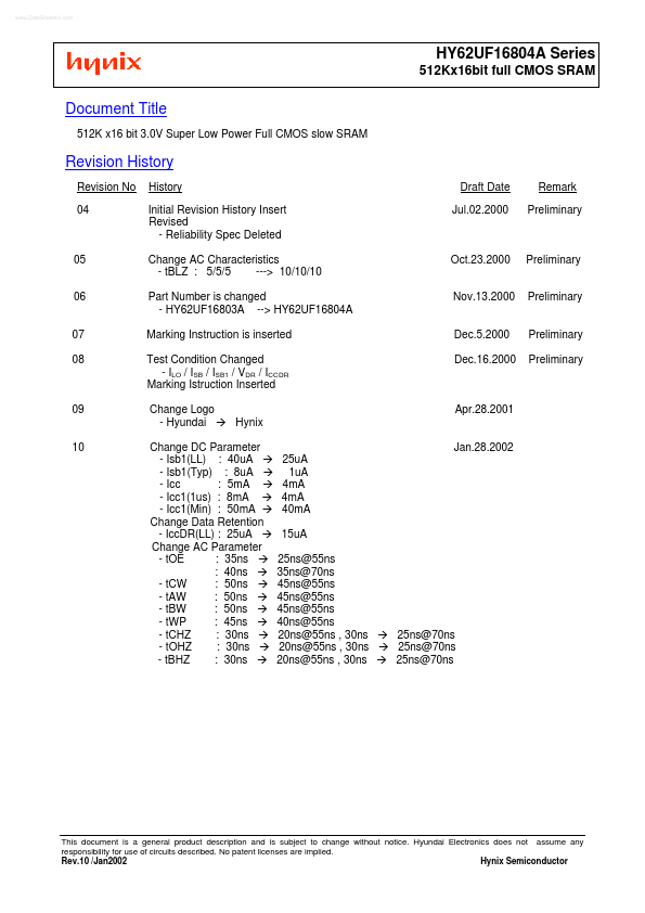
description and is subject to change without notice. Hyundai Electronics does not assume any responsibility for use of circuits described. No patent licenses are implied. Rev.10 /Jan2002 Hynix Semiconductor
DESCRIPTION
The HY62UF16804A is a high speed, super low power and 8Mbit full CMOS SRAM organized as 524,288 words by 16bits. The HY62UF16804A uses high performance full CMOS process technology and is designed for high speed and low power circuit technology. It is particularly wellsuited for the high density low power system application. This device has a data retention mode that guarantees data to remain valid at a minimum power supply voltage of 1.2V. Product Voltage Speed No. (V) (ns) HY62UF16804A-C 2.7~3.3 55/70/85 HY62UF16804A-I 2.7~3.3 55/70/85 Note 1. C : mercial, I : Industrial 2. Current value is max.
FEATURES
- Fully static operation and Tri-state output
- TTL patible inputs and outputs
- Battery backup(LL/SL-part)
- 1.2V(min) data retention
- Standard pin configuration
- 48-u BGA
Operation Current/Icc(m A) 4 4
Standby Current(u A) LL SL 25 8 25 8
Temperature (°C) 0~70 -40~85
PIN CONNECTION ( Top View )
/LB /OE A0 A1 A4 A6 A2 NC
A1,A2 A4,A6~A7 A9 A12 A15~A18 A8
BLOCK DIAGRAM
ADD INPUT BUFFER COLUMN DECODER ROW DECODER SENSE AMP I/O1
IO9 /UB A3 IO10 IO11 A5
/CS IO1 IO2 IO3 IO4 Vcc
I/O8 DATA I/O BUFFER
ADD INPUT BUFFER
PRE DECODER
A10 A13 A14
Vss IO12 A17 A7
MEMORY ARRAY 512K x 16
WRITE DRIVER
I/O9
BLOCK DECODER
Vcc IO13 Vss A16 IO5 Vss IO15 IO14 A14 A15 IO6 IO7 IO16 NC A18 A8 A12 A13 /WE IO8 A9 A10 A11 NC
A0 A3 A5 A11 /CS /OE /LB /UB /WE
ADD INPUT BUFFER
I/O16
PIN DESCRIPTION
Pin Name /CS /WE /OE /LB /UB Pin Function Chip Select Write Enable Output Enable Lower Byte Control(I/O1~I/O8) Upper Byte...