HY5MS7B2BLFP
HY5MS7B2BLFP is Mobile DDR SDRAM manufactured by SK Hynix.
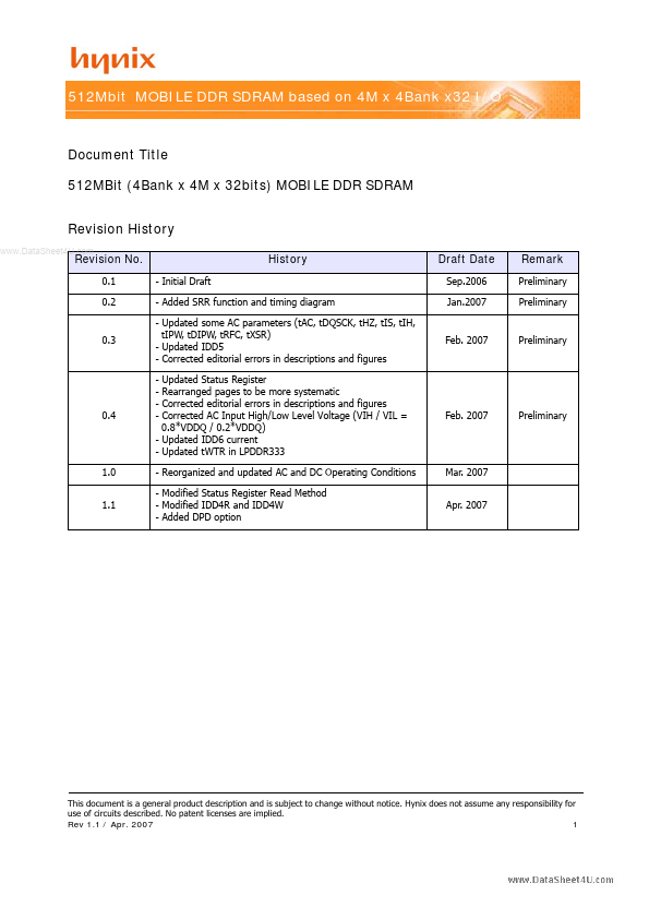
description and is subject to change without notice. Hynix does not assume any responsibility for use of circuits described. No patent licenses are implied. Rev 1.1 / Apr. 2007 1
Mobile DDR SDRAM 512Mbit (16M x 32bit) HY5MS7B2BLF(P) Series FEATURES
SUMMARY
- Mobile DDR SDRAM
- Double data rate architecture: two data transfer per clock cycle
- Mobile DDR SDRAM INTERFACE
- x32 bus width: HY5MS7B2BLFP
..
- MODE RERISTER SET, EXTENDED MODE REGISTER SET and STATUS REGISTER READ
- Keep to the JEDEC Standard regulation (Low Power DDR SDRAM)
- CAS LATENCY
- Programmable CAS latency 2 or 3 supported
- BURST LENGTH
- Multiplexed Address (Row address and Column address)
- SUPPLY VOLTAGE
- 1.8V device: VDD and VDDQ = 1.7V to 1.95V
- MEMORY CELL ARRAY
- 512Mbit (x32 device) = 4M x 4Bank x 32 I/O
- DATA STROBE
- x32 device: DQS0 ~ DQS3
- Bidirectional, data strobe (DQS) is transmitted and received with data, to be used in capturing data at the receiver
- Data and data mask referenced to both edges of DQS
- LOW POWER FEATURES
- PASR (Partial Array Self Refresh)
- AUTO TCSR (Temperature pensated Self Refresh)
- DS (Drive Strength)
- DPD (Deep Power Down): DPD is an optional feature
, so please contact Hynix office for the DPD feature
- INPUT CLOCK
- Differential clock inputs (CK, CK)
- Data MASK
- DM0 ~ DM3: Input mask signals for write data
- DM masks write data-in at the both rising and falling edges of the data strobe
- Programmable burst length 2 / 4 / 8 with both sequential and interleave mode
- AUTO PRECHARGE
- Option for each burst access
- AUTO REFRESH AND SELF REFRESH MODE
- CLOCK STOP MODE
- Clock stop mode is a feature supported by Mobile DDR...