ICS558-02
ICS558-02 is LVHSTL TO CMOS CLOCK DIVIDER manufactured by ICST.
..
LVHSTL TO CMOS CLOCK DIVIDER
Description
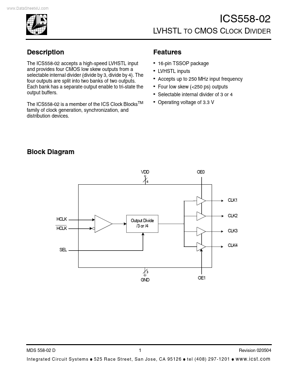
The ICS558-02 accepts a high-speed LVHSTL input and provides four CMOS low skew outputs from a selectable internal divider (divide by 3, divide by 4). The four outputs are split into two banks of two outputs. Each bank has a separate output enable to tri-state the output buffers. The ICS558-02 is a member of the ICS Clock Blocks TM family of clock generation, synchronization, and distribution devices.
Features
- -
- -
- -
16-pin TSSOP package LVHSTL inputs Accepts up to 250 MHz input frequency Four low skew (<250 ps) outputs Selectable internal divider of 3 or 4 Operating voltage of 3.3 V
Block Diagram
OE0
CLK1 CLK2 Output Divide /3 or /4 CLK3 CLK4
HCLK HCLK
OE1
MDS 558-02 D I n t e gra te d C i r c u i t S y s t e m s
- 1
525 Race Stre et, San Jo se, CA 9 5126
- Revision 020504 te l (40 8) 2 97-12 01
- w w w. i c st . c o m
ICS558-02 LVHSTL TO CMOS CLOCK DIVIDER
Pin Assignment
SEL VDD VDD HCLK HCLK GND GND OE0 1 2 3 4 5 6 7 8 16 15 14 13 12 11 10 9 VDD VDD CLK1 CLK2 CLK3 CLK4 GND OE1
Tri-State Table
OE1 0 0 1 1 OE0 0 1 0 1 CLK 1, CLK 2 Tri-state Clock ON Tri-state Clock ON CLK 3, CLK 4 Tri-state Tri-state Clock ON Clock ON
Output Divide Selection
SEL 0 1 Output Divide /3 /4
16 Pin 173 Mil (0.65mm) TSSOP
Pin Descriptions
Pin Number 1 2 3 4 5 6 7 8 9 10 11 12 13 14 15 16 Pin Name SEL VDD VDD HCLK HCLK GND GND OE0 OE1 GND CLK4 CLK3 CLK2 CLK1 VDD VDD Pin Type Input Power Power Input Input Power Power Input Input Power Output Output Output Output Power Power Pin Description Select pin for output divider. See table above. Internal pull-up to VDD. Connect to +3.3 V. Connect to +3.3 V. Differential LVHSTL input (true input). Differential LVHSTL input (plimentary input). Connect to ground. Connect to ground. Output enable for CLK1 and CLK2. See table above. Internal pull-up to VDD. Output enable for CLK3 and CLK4. See table above. Internal pull-up to VDD. Connect...