ICST ICS853210
The ICS853210 is a low skew, high performance dual 1 - t o -5 Differential-to-2.5V/3.3V HiPerClockS™ LVPECL/ECL Fanout Buffer and a member of the HiPerClockS™family of High Performance Clock Solutions from ICS. The ICS853210 is characterized to operate from either a 2.5V or a 3.3V power supply. Guaranteed output and par t-to-par t skew characteristics make the ICS853210 ideal for those clock distribution applications demanding well defined performance and repeatability.| Part No. | ICS853210 |
|---|---|
| Datasheet | ICS853210 Download |
| Manufacturer |  ICST |
| Description | LVPECL/ECL FANOUT BUFFER |
| Buy | Stock & Price |
FEATURES
● 2 differential 2.5V/3.3V LVPECL / ECL bank outputs● 2 differential clock input pairs
● PCLKx, nPCLKx pairs can accept the following differential input levels: LVPECL, LVDS, CML, SSTL
● Maximum output frequency: >3GHz
● Translates any single ended input signal to 3.3V LVPECL levels with resistor bias on nPCLKx input
● Output skew: 13ps (typical)
● Part-to-part skew: 85ps (typical)
● Propagation delay: 485ps (typical)
● LVPECL mode operating voltage supply range: VCC = 2.375V to 3.8V, VEE = 0V
● ECL mode operating voltage supply range: VCC = 0V, VEE = -2.375V to -3.8V
● -40°C to 85°C ambient operating temperature
● Pin compatible with MC100EP210 and MC100LVEP210
GENERAL DESCRIPTION
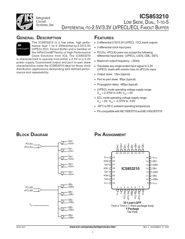
ICS BLOCK DIAGRAM PCLKA nPCLKA QA0 nQA0 QA1 nQA1 QA2 nQA2 QA3 nQA3 QA4 nQA4 PIN ASSIGNMENT nQA3 nQA4 nQB0 nQB1 QA3 QA4 QB0 QB1 24 23 22 21 20 19 18 17 VCCO nQA2 QA2 nQA1 QA1 nQA0 QA0 25 26 27 28 29 30 31 32 1 VCC 16 15 14 VCCO QB2 nQB2 QB3 nQB3 QB4 nQB4 VCCO ICS853210 13 12 11 10 9 nPCLKB PCLKA VBB QB2 nQB2 V BB QB3 nQB3 QB4 nQB4 32-Lead LQFP 7mm x 7mm x 1.4mm package body Y Package Top View 853210AY 1 nPCLKA PCLKB VEE REV.