ICS571
ICS571 is LOW PHASE NOISE ZERO DELAY BUFFER manufactured by IDT.
LOW PHASE NOISE ZERO DELAY BUFFER
Description
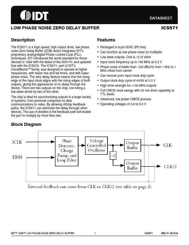
The ICS571 is a high speed, high output drive, low phase noise Zero Delay Buffer (ZDB) which integrates IDT’s proprietary analog/digital Phase Locked Loop (PLL) techniques. IDT introduced the world standard for these devices in 1992 with the debut of the AV9170, and updated that with the ICS570. The ICS571, part of IDT’s Clock Blocks™ family, was designed to operate at higher frequencies, with faster rise and fall times, and with lower phase noise. The zero delay feature means that the rising edge of the input clock aligns with the rising edges of both outputs, giving the appearance of no delay through the device. There are two outputs on the chip, one being a low-skew divide by two of the other.
The chip is ideal for synchronizing outputs in a large variety of systems, from personal puters to data munications to video. By allowing offchip feedback paths, the ICS571 can eliminate the delay through other devices. The use of dividers in the feedback path will enable the part to multiply by more than two.
Features
- Packaged in 8-pin SOIC (Pb free)
- Can function as low phase noise x2 multiplier
- Low skew outputs. One is ÷2 of other
- Input clock frequency up to 160 MHz at 3.3 V
- Phase noise of better than -100 d Bc/Hz from 1 k Hz to 1
MHz offset from carrier
- Can recover poor input clock duty cycle
- Output clock duty cycle of 45/55 at 3.3 V
- High drive strength for >100 MHz outputs
- Full CMOS clock swings with 25 m A drive capability at
TTL levels
- Advanced, low power CMOS process
- Operating voltages of 3.0 to 5.5 V
Block Diagram
IDT™ / ICS™ LOW PHASE NOISE ZERO DELAY BUFFER
REV H 051310
ICS571 LOW PHASE NOISE ZERO DELAY BUFFER
Pin Assignment
ZDB AND MULTIPLIER/DIVIDER
Feedback Configuration Table and Frequency Ranges (at 3.3 V)
Feedback From
CLK CLK/2
Input clock frequency 2x Input clock frequency
CLK/2
Input clock frequency/2 Input clock...