IDT71V67702
IDT71V67702 is Burst Counter Flow-Through Outputs / Single Cycle Deselect manufactured by IDT.
..
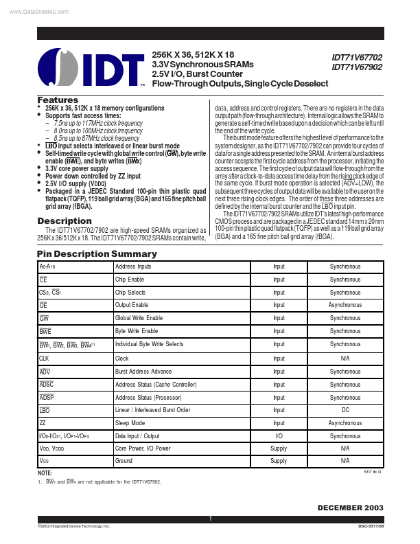
256K X 36, 512K X 18 IDT71V67702 3.3V Synchronous SRAMs IDT71V67902 2.5V I/O, Burst Counter Flow-Through Outputs, Single Cycle Deselect Features x x x x x x x x
256K x 36, 512K x 18 memory configurations Supports fast access times:
- 7.5ns up to 117MHz clock frequency
- 8.0ns up to 100MHz clock frequency
- 8.5ns up to 87MHz clock frequency LBO input selects interleaved or linear burst mode Self-timed write cycle with global write control (GW), byte write enable (BWE), and byte writes (BWx) 3.3V core power supply Power down controlled by ZZ input 2.5V I/O supply (VDDQ) Packaged in a JEDEC Standard 100-pin thin plastic quad flatpack (TQFP), 119 ball grid array (BGA) and 165 fine pitch ball grid array (f BGA).
Description
The IDT71V67702/7902 are high-speed SRAMs organized as 256K x 36/512K x 18. The IDT71V67702/7902 SRAMs contain write, data, address and control registers. There are no registers in the data output path (flow-through architecture). Internal logic allows the SRAM to generate a self-timed write based upon a decision which can be left until the end of the write cycle. The burst mode feature offers the highest level of performance to the system designer, as the IDT71V67702/7902 can provide four cycles of data for a single address presented to the SRAM. An internal burst address counter accepts the first cycle address from the processor, initiating the access sequence. The first cycle of output data will flow-through from the array after a clock-to-data access time delay from the rising clock edge of the same cycle. If burst mode operation is selected (ADV=LOW), the subsequent three cycles of output data will be available to the user on the next three rising clock edges. The order of these three addresses are defined by the internal burst counter and the LBO input pin. The IDT71V67702/7902 SRAMs utilize IDT’s latest high-performance CMOS process and are packaged in a JEDEC standard 14mm x 20mm 100-pin thin plastic quad flatpack...


