Inchange Semiconductor 10N80
The information contained herein is presented only as a guide for the applications of our products. The products are not designed for use in equipment which require specialized quality and/or reliability, or in equipment which could have applications in hazardous environments, aerospace industry, or medical field.| Part No. | 10N80 |
|---|---|
| Datasheet | 10N80 Download |
| Manufacturer |  Inchange Semiconductor |
| Description | N-Channel MOSFET |
| Buy | Stock & Price |
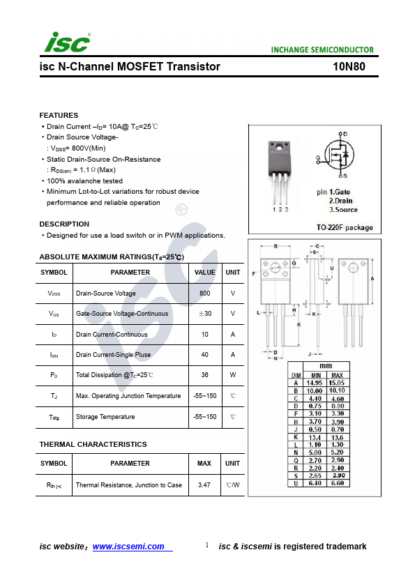
FEATURES
●Drain Current –ID= 10A@ TC=25℃●Drain Source Voltage- : VDSS= 800V(Min)
●Static Drain-Source On-Resistance : RDS(on) = 1.1Ω(Max)
●100% avalanche tested
●Minimum Lot-to-Lot variations for robust device performance and reliable operation
DESCRIPTION
●Designed for use a load switch or in PWM applications.ABSOLUTE MAXIMUM RATINGS
(Ta=25℃) SYMBOL PARAMETER VALUE UNIT VDSS Drain-Source Voltage 800 V VGS Gate-Source Voltage-Continuous ID Drain Current-Continuous ±30 V 10 A IDM Drain Current-Single Pluse PD Total Dissipation @TC=25℃ 40 A 36 W TJ Max. Operating Junction Temperature -55~150 ℃ Tstg Storage Temperature -55~150 ℃ THERMAL CHARACTERISTICS SYMBOL PARAMETER MAX UNIT Rth j-c Thermal Resistance, Junction to Case 3.47 ℃/W 10N80 isc website: 1 isc & iscsemi is registered trademark isc N-Channel MOSFET TransistorELECTRICAL CHARACTERISTICS
TC=25℃ unless otherwise specified SYMBOL PARAMETER CONDITIONS V(BR)DSS Drain-Source Breakdown Voltage VGS= 0; ID= 0.25mA VGS(th) Gate Threshold...