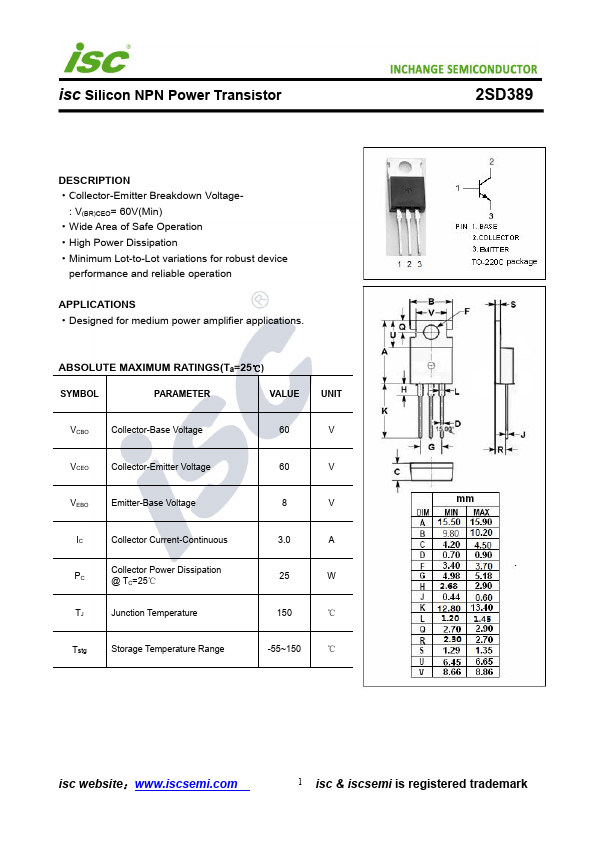
2SD389
DESCRIPTION
- Collector-Emitter Breakdown Voltage-
: V(BR)CEO= 60V(Min)
- Wide Area of Safe Operation
- High Power Dissipation
- Minimum Lot-to-Lot variations for robust device performance and reliable operation
APPLICATIONS
- Designed for medium power amplifier applications.
ABSOLUTE MAXIMUM RATINGS(Ta=25℃)
SYMBOL
PARAMETER
VALUE
UNIT
VCBO
Collector-Base Voltage
VCEO
Collector-Emitter Voltage
VEBO
Emitter-Base Voltage
Collector Current-Continuous
Collector Power Dissipation @ TC=25℃
Junction Temperature
℃
Tstg
Storage Temperature Range
-55~150
℃
2SD389 isc website:.iscsemi.
1 isc & iscsemi is registered trademark isc Silicon NPN Power Transistor
ELECTRICAL CHARACTERISTICS
TC=25℃ unless otherwise specified
SYMBOL
PARAMETER...