BFP196W Overview
Key Specifications
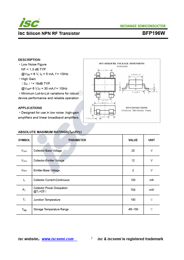
Package: SOT
Mount Type: Surface Mount
Pins: 4
Max Frequency: 7.5 GHz
Description
Low Noise Figure NF = 1.3 dB TYP. @VCE = 6 V, IC = 5 mA, f = 1GHz - High Gain ︱S21︱2 = 18dB TYP.
| Part | BFP196W |
|---|---|
| Description | NPN Transistor |
| Category | Transistor |
| Manufacturer | Inchange Semiconductor |
| Size | 216.43 KB |
Package: SOT
Mount Type: Surface Mount
Pins: 4
Max Frequency: 7.5 GHz
Low Noise Figure NF = 1.3 dB TYP. @VCE = 6 V, IC = 5 mA, f = 1GHz - High Gain ︱S21︱2 = 18dB TYP.
| Seller | Inventory | Price Breaks | Buy |
|---|---|---|---|
| Avnet | 3000 | 3000+ : 0.08952 USD 6000+ : 0.08726 USD 12000+ : 0.08501 USD 24000+ : 0.08275 USD |
View Offer |
| Avnet | 2610 | 1+ : 0.324 USD 10+ : 0.218 USD 25+ : 0.206 USD 50+ : 0.195 USD |
View Offer |
| Part Number | Manufacturer | Description |
|---|---|---|
| BFP196W | Siemens Semiconductor Group | NPN Silicon RF Transistor |
| BFP196W | Infineon | Low Noise Silicon Bipolar RF Transistor |
| BFP196 | Infineon | Low Noise Silicon Bipolar RF Transistor |
| BFP196 | Siemens Semiconductor Group | NPN Silicon RF Transistor |
| BFP193TW | Vishay | Silicon NPN Planar RF Transistor |