IXTA1N100P
Key Features
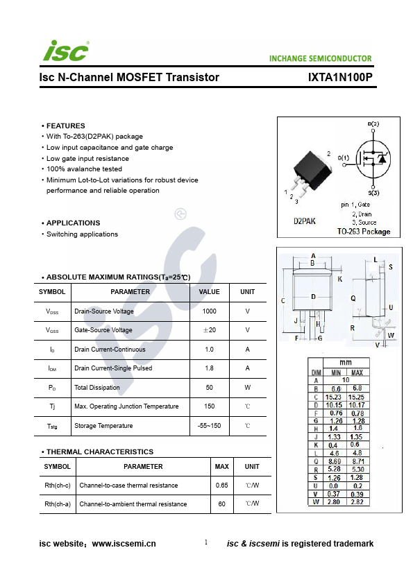
- With To-263(D2PAK) package
- Low input capacitance and gate charge
- Low gate input resistance
- 100% avalanche tested
- Minimum Lot-to-Lot variations for robust device performance and reliable operation
| Part Number | Manufacturer | Description |
|---|---|---|
| IXTA1N100P | IXYS | Power MOSFET |