UTT50N06L-TA3
UTT50N06L-TA3 is N-Channel MOSFET manufactured by Inchange Semiconductor.
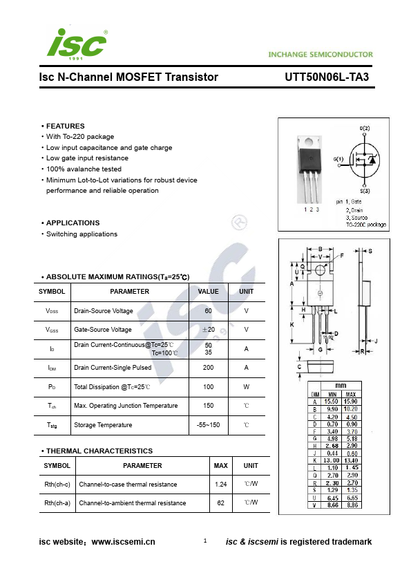
Isc N-Channel MOSFET Transistor
- Features
- With To-220 package
- Low input capacitance and gate charge
- Low gate input resistance
- 100% avalanche tested
- Minimum Lot-to-Lot variations for robust device performance and reliable operation
- APPLICATIONS
- Switching applications
-...