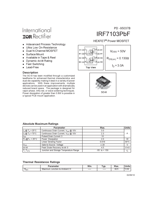
DESCRIPTION
The package is designed for vapor phase, infra red, or wave soldering techniques. Power dissipation of greater than 0.8W is possible in a typical PCB mount application. SO-8 ABSOLUTE MAXIMUM RATINGS
ID @ TA = 25°C ID @ TA = 70°C IDM PD @TA = 25°C VGS dv/dt TJ, TSTG Parameter Continuous Drain Current, VGS @ 10V Continuous Drain Current, VGS @ 10V Pulsed Drain Current Power Dissipation Linear Derating Factor Gate-to-Source Voltage Peak Diode Recovery dv/dt Junction and Storage Temperature Range Max. 3.0 2.3 10 2.0 0.016 ± 20 4.5 -55 to + 150 Units A W W/°C V V/nS °C Thermal Resistance Ratings Parameter RθJA Maximum Junction-to-Ambient Min. Typ. Max. 62.5 Units °C/W 02/09/10 IRF7103PbF ELECTRICAL CHARACTERISTICS
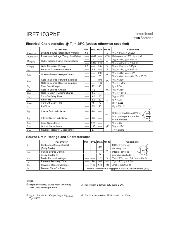
@ TJ = 25°C (unless otherwise specified) Parameter Min. Typ. Max. Units Conditions V(BR)DSS Drain-to-Source Breakdown Voltage 50 V VGS = 0V, ID = 250µA ∆V(BR)DSS/∆TJ Breakdown Voltage Temp. Coefficient RDS(ON) Static Drain-to-Source On-Resistance... International Rectifier