International Rectifier IRF7380
Power MOSFET
| Part No. | IRF7380 |
|---|---|
| Datasheet | IRF7380 Download |
| Manufacturer |  International Rectifier |
| Description | Power MOSFET |
| Buy | Stock & Price |
APPLICATIONS
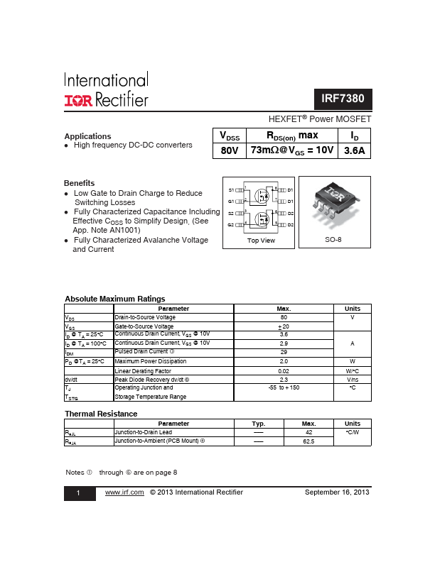
High frequency DC-DC converters VDSS 80V RDS(on) max 73mΩ@VGS = 10V ID 3.6A Benefits Low Gate to Drain Charge to Reduce Switching Losses Fully Characterized Capacitance Including Effective COSS to Simplify Design, (See App. Note AN1001) Fully Characterized Avalanche Voltage and Current S1 G1 S2 G2 1 8 D1 D1 D2 D2 2 7 3 6 4 5 Top View SO-8ABSOLUTE MAXIMUM RATINGS
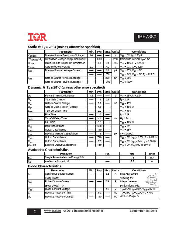
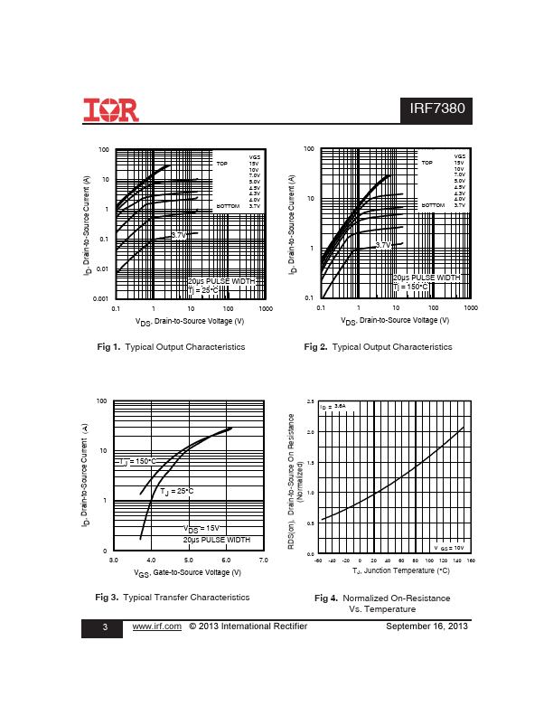
Parameter VDS VGS ID @ TA = 25°C ID @ TA = 100°C IDM PD @TA = 25°C dv/dt TJ TSTG Drain-to-Source Voltage Gate-to-Source Voltage Continuous Drain Current, VGS @ 10V Continuous Drain Current, VGS @ 10V Pulsed Drain Current Maximum Power Dissipation Linear Derating Factor Peak Diode Recovery dv/dt Operating Junction and Storage Temperature Range Max. 80 ± 20 3.6 2.9 29 2.0 0.02 2.3 -55 to + 150 Units V A W W/°C V/ns °C Thermal Resistance Parameter RθJL RθJA Junction-to-Drain Lead Junction-to-Ambient (PCB Mount) * Typ. ––– ––– Max. 20 50 Units °C/W Notes through are on page 8 1 08/28/02 IRF7380 Static @ TJ = 25°C (unless otherwise specified) Parameter V(BR)DSS ∆V(BR)DSS/∆TJ RDS(on) VGS(th) IDSS IGSS Drain-to-Source Breakdown Voltage Breakdown Voltage Temp.