IS46DR81280DL
FEATURES
- Standard Voltage: Vdd and Vddq = 1.8V ±0.1V
- Low Voltage (L): Vdd and Vddq = 1.5V ±0.075V
- SSTL_18-patible for Standard Voltage
- SSTL_15-patible for Low Voltage
- Double data rate interface: two data transfers per clock cycle
- Differential data strobe (DQS, DQS)
- 4-bit prefetch architecture
- On chip DLL to align DQ and DQS transitions with CK
- 8 internal banks for concurrent operation
- Programmable CAS latency (CL) 3, 4, 5, 6 and 7 sup- ported
- Programmable CAS latency (CL) 3, 4, 5, 6, 7, 8 and 9 supported
- Posted CAS and programmable additive latency (AL)
0, 1, 2, 3, 4, 5 and 6 supported
- WRITE latency = READ latency
- 1 t CK
- Programmable burst lengths: 4 or 8
- Adjustable data-output drive strength, full and reduced strength options
- On-die termination (ODT)
OPTIONS
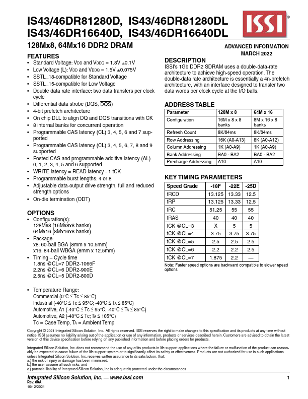
- Configuration(s): 128Mx8 (16Mx8x8 banks) 64Mx16 (8Mx16x8 banks)
- Package: x8: 60-ball BGA (8mm x 10.5mm) x16: 84-ball WBGA (8mm x 12.5mm)
- Timing
- Cycle time 1.8ns @CL=7 DDR2-1066F 2.2ns...