180N10
Overview
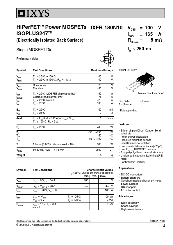
- Silicon chip on Direct-Copper-Bond substrate - High power dissipation - Isolated mounting surface - 2500V electrical isolation
- Low drain to tab capacitance(<25pF)
- Low RDS (on) HDMOSTM process
- Rugged polysilicon gate cell structure
- Unclamped Inductive Switching (UIS) rated
- Fast intrinsic Rectifier