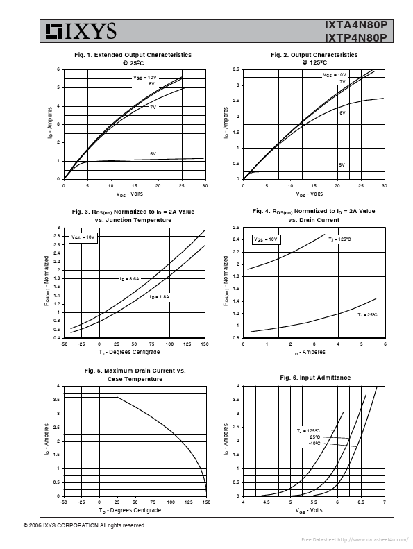
z z
Symbol Test Conditions (TJ = 25°C, unless otherwise specified) BVDSS VGS(th) IGSS IDSS RDS(on) VGS = 0 V, ID = 250 μA VDS = VGS, ID = 100μA VGS = ±30 V, VDS = 0 V VDS = VDSS VGS = 0 V TJ = 125°C
Characteristic Values Min. Typ. Max. 800 3.0 5.5 ±100 5 150 3.4 V V nA μA μA Ω
z
International standard packages Unclamped Inductive Switching (UIS) rated Low package inductance - easy to drive and to protect
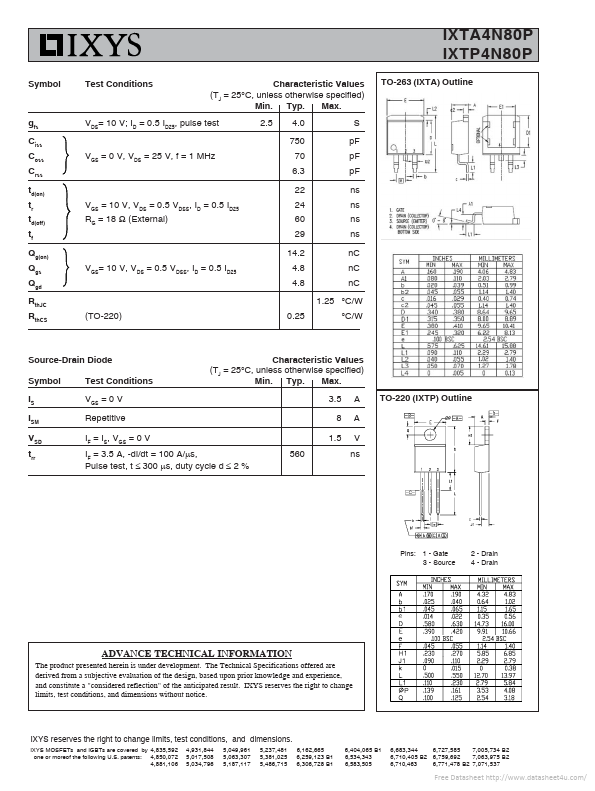
Advantages
z z z
Easy to mount Space savings High power density
VGS = 10 V, ID = 0.5.
Full PDF Text Transcription for IXTP4N80P (Reference)
Note: Below is a high-fidelity text extraction (approx. 800 characters) for
IXTP4N80P. For precise diagrams, and layout, please refer to the original PDF.
Advance Technical Information PolarHVTM Power MOSFET N-Channel Enhancement Mode Avalanche Rated IXTA4N80P IXTP4N80P VDSS = 800 = 3.6 ID25 RDS(on) ≤ 3.4 V A Ω Symbol VDSS ...
View more extracted text
4N80P IXTP4N80P VDSS = 800 = 3.6 ID25 RDS(on) ≤ 3.4 V A Ω Symbol VDSS VDGR VGSS VGSM ID25 IDM IAR EAR EAS dv/dt PD TJ TJM Tstg TL TSOLD Md Weight Test Conditions TJ = 25°C to 150°C TJ = 25°C to 150°C; RGS = 1 MΩ Continuous Transient TC = 25°C TC = 25°C, pulse width limited by TJM TC = 25°C TC = 25°C TC = 25°C IS ≤ IDM, di/dt ≤ 100 A/μs, VDD ≤ VDSS, TJ ≤ 150°C, RG = 18 Ω TC = 25°C Maximum Ratings 800 V 800 V ± 30 ± 40 3.6 8 2 20 250 10 100 -55 ... +150 150 -55 ... +150 V V A A A mJ mJ V/ns W °C °C °C TO-263 (IXTA) G S (TAB) TO-220 (IXTP) G D S (TAB) G = Gate S = Source D = Drain TAB = Drain 1.6 mm (0.062 in.