Description
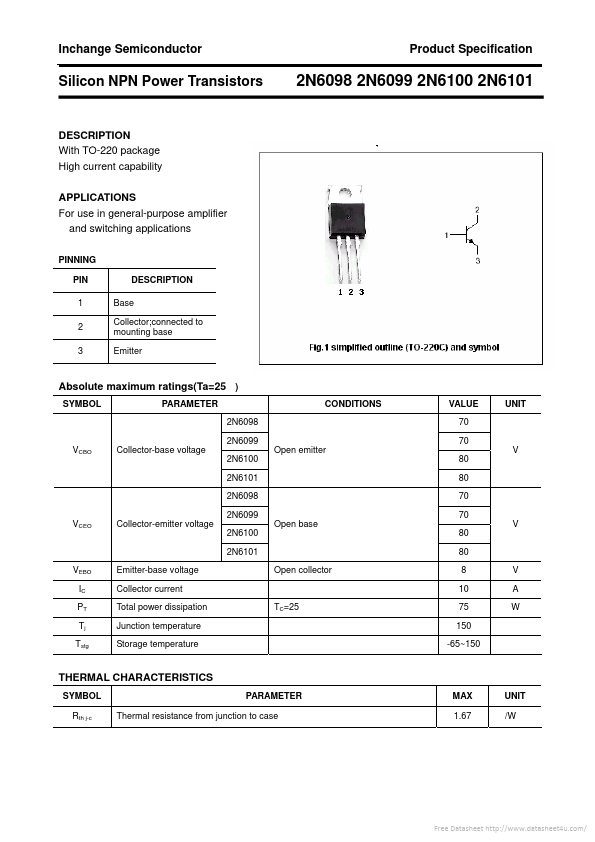
¡¤With TO-220 package ¡¤High current capability APPLICATIONS ¡¤For use in general-purpose amplifier and switching applications PINNING PIN 1 2 3 DESCRIPTION Base Collector;connected to mounting base Emitter SYMBOL PARAMETER 2N6098 2N6099 VCBO Collector-base voltage 2N6100 2N6101 2N6098 2N6099 VCEO Collector-emitter voltage 2N6100 2N6101 VEBO IC PT Tj Tstg Emitter-base voltage Collector current Total power dissipation Junction temperature Storage temperature TC=25¡æ Open collector Open base 80 80 8 10 75 150 -65~150 ¡æ ¡æ V A W Open emitter 80 80 70 70 V CONDITIONS VALUE 70 70 V UNIT SYMBOL Rth j-c PARAMETER Free Datasheet Inchange Semiconductor Product Specification Silicon NPN Power Transistors CHARACTERISTICS Tj=25¡æ unless otherwise specified PARAMETER 2N6098 2N6099 VCEO(SUS) Collector-emitter sustaining voltage 2N6100 2N6101 VCEsat-1 VCEsat-2 Collector-emitter saturation voltage Collector-emitter saturation voltage 2N6098/6099 VBE Base-emitter on voltage 2N6100/6101 ICBO IEBO Collector cut-off current Emitter cut-off current 2N6098/6099 hFE DC current gain 2N6100/6101 fT Transition frequency 2N6098 2N6099 2N6100 2N6101 SYMBOL CONDITIONS MIN 70 70 TYP. MAX UNIT IC=0.1A ;IB=0 80 80 IC=5A;IB=0.5A IC=10A;IB=2.5A IC=4A ; VCE=4V 1.3 IC=5A ; VCE=4V VCB=Rated VCBO;IE=0 TC=150¡æ VEB=8V; IC=0 IC=4A ; VCE=4V 20 IC=5A ; VCE=4V IC=1A ; VCE=10V 0.8 80 0.5 2.0 1.0 1.3 3.5 V V V V mA mA MHz 2 Free Datasheet Inchange Semiconductor Product Specification Silicon NPN Power Transistors PACKAGE OUTLINE 2N6098 2N6099 2N6100 2N6101 Fig.2 Outline dimensions(unindicated tolerance:¡À 0.10 mm) 3 Free Datasheet.