2N6490
DESCRIPTION
With TO-220 package Excellent safe operating area plement to type 2N6486 2N6487
2N6488 respectively
APPLICATIONS Power amplifier and medium speed switching applications
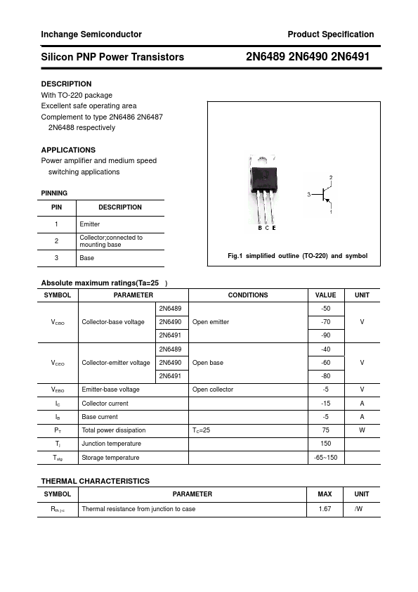
PINNING PIN
DESCRIPTION
1 Emitter
Collector;connected to mounting base
3 Base
Fig.1 simplified outline (TO-220) and symbol
Absolute maximum ratings(Ta=25 )
SYMBOL
PARAMETER
2N6489
VCBO
Collector-base voltage 2N6490
2N6491
2N6489
VCEO
Collector-emitter voltage 2N6490
2N6491
VEBO
Emitter-base voltage
IC Collector current
IB Base current
PT Total power dissipation
Tj Junction temperature
Tstg Storage temperature
CONDITIONS Open emitter
Open base Open collector
TC=25
THERMAL CHARACTERISTICS
SYMBOL
PARAMETER
Rth j-c
Thermal resistance from junction to case
VALUE -50 -70 -90 -40 -60 -80 -5 -15 -5 75 150
-65~150
UNIT...