BTS149
BTS149 is Smart Lowside Power Switch manufactured by Infineon.
Features
- Logic Level Input
- Input Protection (ESD)
- =Thermal shutdown with latch
- Overload protection
- Short circuit protection
- Overvoltage protection
- Current
Product Summary Drain source voltage On-state resistance Current limit Nominal load current Clamping energy VDS RDS(on) I D(lim) I D(ISO) EAS 60 18 30 19 V mΩ A A
6000 m J limitation
- Status feedback with external input resistor
- Analog driving possible
Application
- All kinds of resistive, inductive and capacitive loads in switching or linear applications
- µC patible power switch for 12 V and 24 V DC applications
- Replaces electromechanical relays and discrete circuits
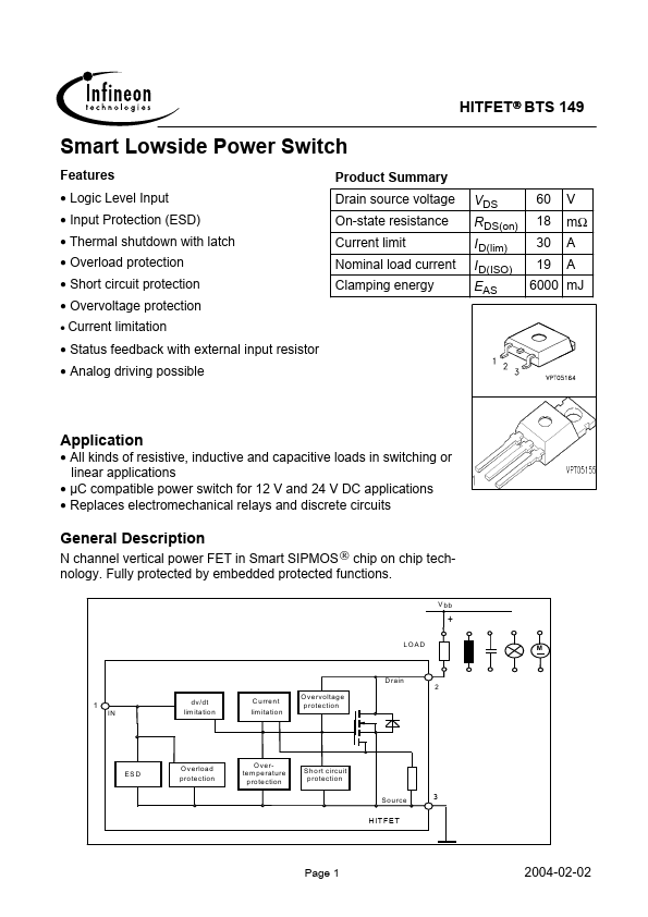
General Description
N channel vertical power FET in Smart SIPMOS chip on chip technology. Fully protected by embedded protected functions.
V bb
+
LOAD
D rain
IN dv /d t lim ita tio n
C u rre n t lim ita tio n
O ve rvoltag e p rotection
O v erloa d pro te ctio n
O ve rte m pe rature p ro te ctio n
Sh ho rt circ c ircu it S ort uit p protection ro te ctio n
S o u rce
H IT F E T
Page 1
2004-02-02
BTS 149
Maximum Ratings at Tj = 25 °C unless otherwise specified Parameter Drain source voltage Drain source voltage for short circuit protection Continuous input current 1) -0.2V ≤ VIN ≤ 10V VIN < -0.2V or VIN > 10V Operating temperature Storage temperature Power dissipation TC = 25 °C Unclamped single pulse inductive energy ID(ISO) = 19 A Electrostatic discharge voltage (Human Body Model) VESD according to MIL STD 883D, method 3015.7 and EOS/ESD assn. standard S5.1
- 1993 Load dump protection VLoad Dump2) = VA + VS VIN=low or high; VA =13.5 V td = 400 ms, RI = 2 Ω, ID =0,5- 19A td = 400 ms, RI = 2 Ω, ID = 19A DIN humidity category, DIN 40 040 IEC climatic category; DIN IEC 68-1 VLD 110 92 E 40/150/56 3000 V EAS 6000 m J Tj Tstg Ptot Symbol VDS VDS(SC) IIN no limit | IIN | ≤...