Infineon Technologies BAR81
Silicon RF Switching Diodes
| Part No. | BAR81 |
|---|---|
| Datasheet | BAR81 Download |
| Manufacturer |  Infineon Technologies |
| Description | Silicon RF Switching Diodes |
| Buy | Stock & Price |
MAXIMUM RATINGS
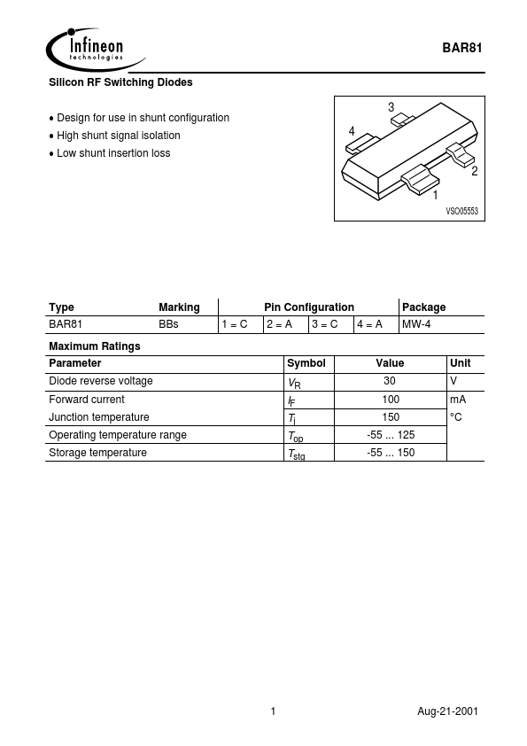
Parameter Diode reverse voltage Forward current Junction temperature Marking BBs 1=C Pin Configuration 2=A 3=C 4=A Package MW-4 Symbol VR IF Tj Top Tstg Value 30 100 150 -55 ... 125 -55 ... 150 Unit V mA °C Operating temperature range Storage temperature 1 Aug-21-2001 BAR81ELECTRICAL CHARACTERISTICS
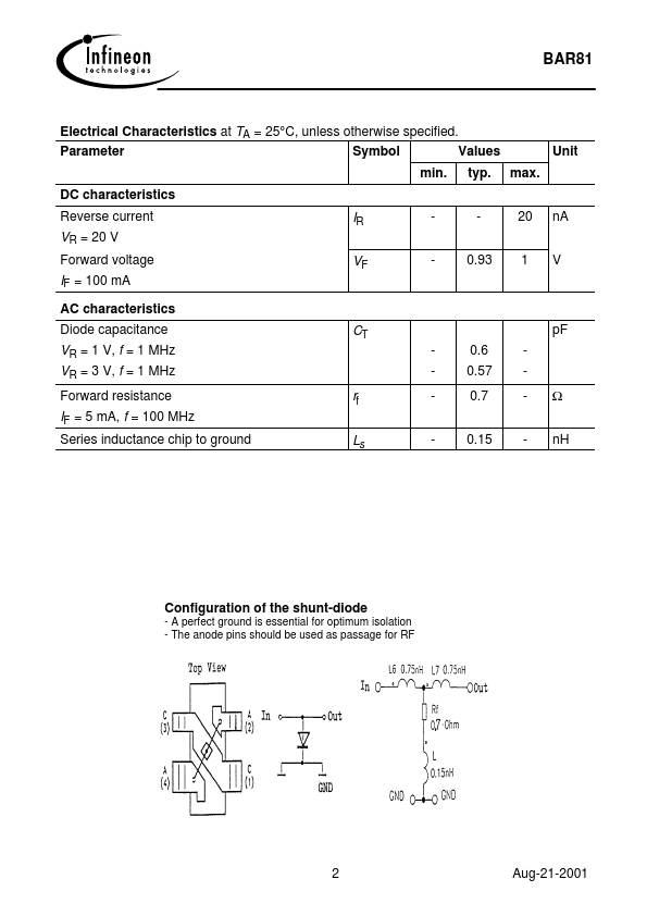
at TA = 25°C, unless otherwise specified. Parameter Symbol Values min. DC characteristics Reverse current VR = 20 V Forward voltage IF = 100 mA VF 0.93 1 IR 20 typ. max. Unit nA V AC characteristics Diode capacitance VR = 1 V, f = 1 MHz VR = 3 V, f = 1 MHz Forward resistance IF = 5 mA, f = 100 MHz Series inductance chip to ground Ls 0.15 nH rf CT 0.6 0.57 0.7 pF Configuration of the shunt-diode - A perfect ground is essential for optimum isolation - The anode pins should be used as passage for RF 2 Aug-21-2001