ICS831752I
ICS831752I is Clock Switch manufactured by Integrated Device Technology.
Clock Switch for ATCA/AMC and PCIe Applications
DATA SHEET
General Description
The ICS831752I is a high-performance, differential HCSL clock switch. The device is designed for the routing of PCIe clock signals in ATCA/AMC system and is optimized for PCIe Gen 1, Gen 2 and Gen 3. The device has one differential, bi-directional I/O (FCLK) for connection to ATCA clock sources and to clock receivers through a connector. The differential clock input CLK is the local clock input and the HCSL output Q is the local clock output. In the mon clock mode, FCLK serves as an input and is routed to the differential HCSL output Q. There are two local clock modes. In the local clock mode 0, CLK is the input, Q is the clock output and FCLK is in high-impedance state. In the local clock mode 1, CLK is the input and both Q and FCLK are the outputs of the locally generated PCIe clock signal. The ICS831752I is characterized to operate from a 3.3V power or 2.5V power supply. The ICS831752I supports the switching of PCI Express (2.5 Gb/s), Gen 2 (5 Gb/s) and Gen 3 (8 Gb/s) clock signals.
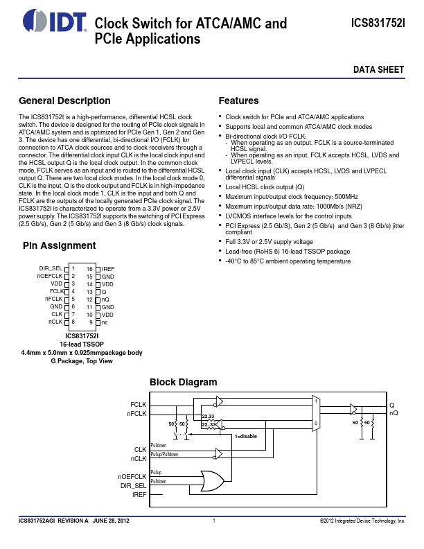
Pin Assignment
DIR_SEL n OEFCLK
VDD FCLK n FCLK GND CLK n CLK
1 2 3 4 5 6 7 8
16 IREF 15 GND 14 VDD 13 Q 12 n Q 11 GND 10 VDD
9 nc
ICS831752I 16-lead TSSOP 4.4mm x 5.0mm x 0.925mmpackage body G Package, Top View
Features
- Clock switch for PCIe and ATCA/AMC applications
- Supports local and mon ATCA/AMC clock modes
- Bi-directional clock I/O FCLK:
- When operating as an output, FCLK is a source-terminated HCSL signal.
- When operating as an input, FCLK accepts HCSL, LVDS and LVPECL levels.
- Local clock input (CLK) accepts HCSL, LVDS and LVPECL differential signals
- Local HCSL clock output (Q)
- Maximum input/output clock frequency: 500MHz
- Maximum input/output data rate: 1000Mb/s (NRZ)
- LVCMOS interface levels for the control inputs
- PCI Express (2.5 Gb/S), Gen 2 (5 Gb/s) and Gen 3 (8 Gb/s) jitter pliant
- Full 3.3V or 2.5V supply voltage
- Lead-free (Ro HS 6) 16-lead TSSOP...