IDT23S09E Overview
Key Specifications
Package: SOP
Mount Type: Surface Mount
Operating Voltage: 3.3 V
Max Voltage (typical range): 3.6 V
Key Features
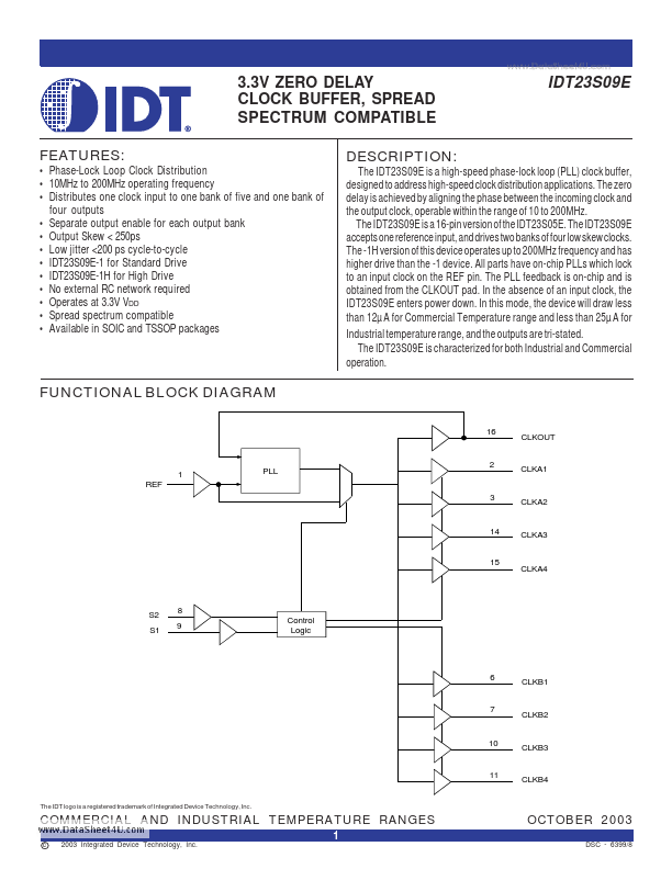
- Phase-Lock Loop Clock Distribution
- 10MHz to 200MHz operating frequency
| Part | IDT23S09E |
|---|---|
| Description | 3.3V ZERO DELAY CLOCK BUFFER |
| Manufacturer | Integrated Device Technology |
| Size | 83.64 KB |
Package: SOP
Mount Type: Surface Mount
Operating Voltage: 3.3 V
Max Voltage (typical range): 3.6 V
| Seller | Inventory | Price Breaks | Buy |
|---|---|---|---|
| Component Stockers USA | 507 | 1+ : 99.99 USD | View Offer |
| Worldway Electronics | 11580 | - | View Offer |
| Part Number | Manufacturer | Description |
|---|---|---|
| IDT23S09E | Renesas | 3.3V ZERO DELAY CLOCK BUFFER |
| IDT23S09 | Integrated Device | IDT23S09 3.3V ZERO DELAY CLOCK BUFFER |
| IDT23S09 | Renesas | 3.3V ZERO DELAY CLOCK BUFFER |
| IDT23S05E | Integrated Device | 3.3V ZERO DELAY CLOCK BUFFER |
| IDT23S08T | Renesas | 2.5V ZERO DELAY CLOCK MULTIPLIER |