IDT72V7290
Overview
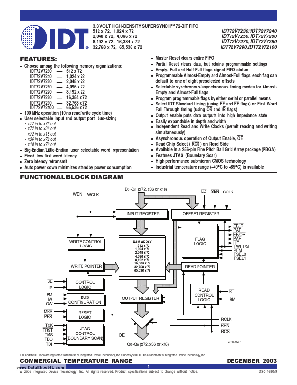
- Choose among the following memory organizations: IDT72V7230 512 x 72 IDT72V7240 1,024 x 72 IDT72V7250 2,048 x 72 IDT72V7260 4,096 x 72 IDT72V7270 8,192 x 72 IDT72V7280 16,384 x 72 IDT72V7290 32,768 x 72 IDT72V72100 65,536 x 72 100 MHz operation (10 ns read/write cycle time) User selectable input and output port bus-sizing - x72 in to x72 out - x72 in to x36 out - x72 in to x18 out - x36 in to x72 out - x18 in to x72 out Big-Endian/Little-Endian user selectable word representation Fixed, low first word latency Zero latency retransmit Auto power down minimizes standby power consumption * * * * * * * * * * * * * * *
- Master Reset clears entire FIFO Partial Reset clears data, but retains programmable settings Empty, Full and Half-Full flags signal FIFO status Programmable Almost-Empty and Almost-Full flags, each flag can default to one of eight preselected offsets Selectable synchronous/asynchronous timing modes for AlmostEmpty and Almost-Full flags Program programmable flags by either serial or parallel means Select IDT Standard timing (using EF and FF flags) or First Word Fall Through timing (using OR and IR flags) Output enable puts data outputs into high impedance state Easily expandable in depth and width Independent Read and Write Clocks (permit reading and writing simultaneously) Asynchronous operation of Output Enable, OE Read Chip Select ( RCS ) on Read Side Available in a 256-pin Fine Pitch Ball Grid Array package (PBGA) Features JTAG (Boundary Scan) High-performance submicron CMOS technology Industrial temperature range (-40°C to +85°C) is available