IS42S16400D
IS42S16400D is 1 Meg Bits x 16 Bits x 4 Banks SYNCHRONOUS DYNAMIC RAM manufactured by ISSI.
1 Meg Bits x 16 Bits x 4 Banks (64-MBIT) SYNCHRONOUS DYNAMIC RAM
Features
- Clock frequency: 166, 143 MHz
- Fully synchronous; all signals referenced to a positive clock edge
- Internal bank for hiding row access/precharge
- Single 3.3V power supply
..
- LVTTL interface
ISSI
JULY 2006
®
OVERVIEW ISSI's 64Mb Synchronous DRAM IS42S16400D is organized as 1,048,576 bits x 16-bit x 4-bank for improved performance. The synchronous DRAMs achieve high-speed data transfer using pipeline architecture. All inputs and outputs signals refer to the rising edge of the clock input.
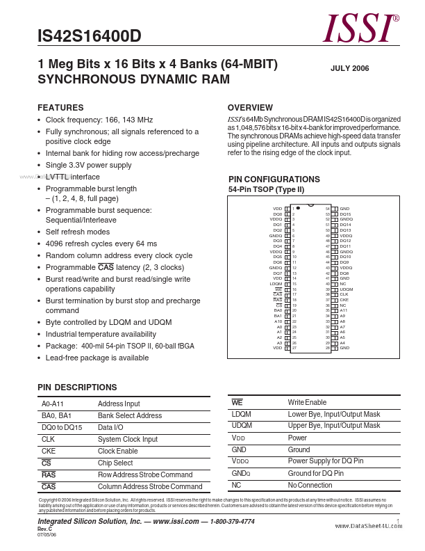
PIN CONFIGURATIONS
54-Pin TSOP (Type II)
VDD DQ0 VDDQ DQ1 DQ2 GNDQ DQ3 DQ4 VDDQ DQ5 DQ6 GNDQ...