Download IR2110E4 Datasheet PDF
International Rectifier
IR2110E4
IR2110E4 is HIGH AND LOW SIDE DRIVER manufactured by International Rectifier.
Features n Floating channel designed for bootstrap operation Fully operational to +400V Tolerant to negative transient voltage d V/dt immune n Gate drive supply range from 10 to 20V n Undervoltage lockout for both channels n Separate logic supply range from 5 to 20V Logic and power ground ±5V offset n CMOS Schmitt-triggered inputs with pull-down n Cycle by cycle edge-triggered shutdown logic n Matched propagation delay for both channels n Outputs in phase with inputs HIGH AND LOW SIDE DRIVER Product Summary VOFFSET 400V max. IO+/- 2A / 2A VOUT - 20V ton/off (typ.) 120ns & 94ns Delay Matching 10ns Description 
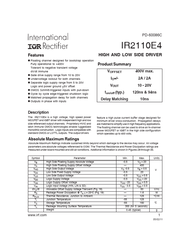
The IR2110E4 is a high voltage, high speed power MOSFET and IGBT driver with independent high and low side referenced output channels. Proprietary HVIC and latch immune CMOS technologies enable ruggedized monolithic construction. Logic inputs are patible with standard CMOS or LSTTL outputs. The output drivers feature a high pulse current buffer stage designed for minimum driver cross-conduction. Propagation delays are matched to simplify use in high frequency applications. The floating channel can be used to drive an N-channel power MOSFET or IGBT in the high side configuration which operates up to 400 volts. Absolute Maximum Ratings Absolute Maximum Ratings indicate sustained limits beyond which damage to the device may occur. All voltage parameters are absolute voltages referenced to . The Thermal Resistance and Power Dissipation ratings are measured under board mounted and still air conditions. Additional information is shown in Figures 28 through 35. Symbol VB VS VHO VCC VLO VDD VSS VIN d VS/dt PD Rth JA Tj TS TL Parameter High Side Floating Supply Absolute Voltage High Side Floating Supply Offset Voltage High Side Output Voltage Low Side Fixed Supply Voltage Low Side Output Voltage Logic Supply Voltage Logic Supply Offset Voltage Logic Input Voltage (HIN, LIN & SD) Allowable Offset Supply Voltage Transient (Fig. 16) Package Power...