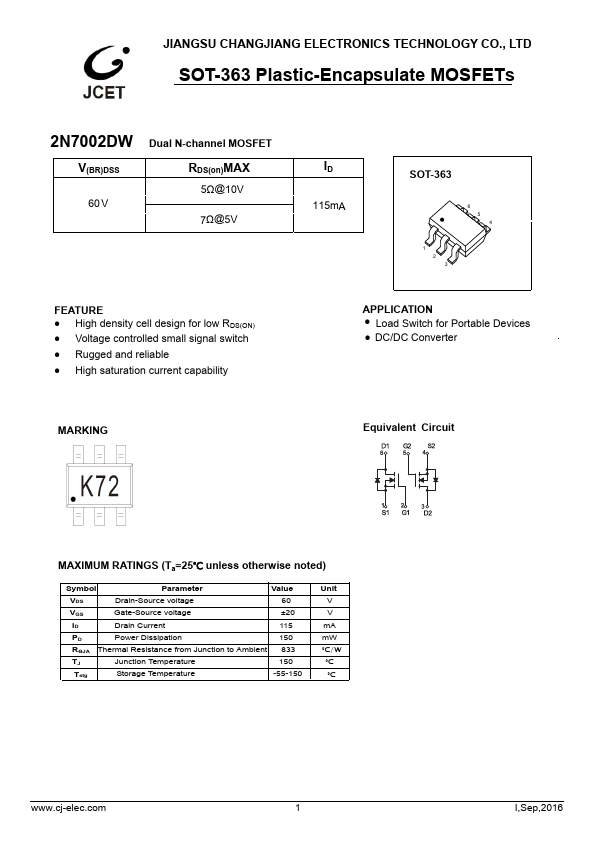
MAXIMUM RATINGS
(Ta=25℃ unless otherwise noted) Symbol Parameter Value VDS Drain-Source voltage 60 VGS Gate-Source voltage ±20 ID Drain Current 115 PD Power Dissipation 150 RӨJA Thermal Resistance from Junction to Ambient 833 TJ Junction Temperature 150 Tstg Storage Temperature -55-150 Unit V V mA mW ℃/W ℃ ℃ 1 I,Sep,2016 MOSFET ELECTRICAL CHARACTERISTICS
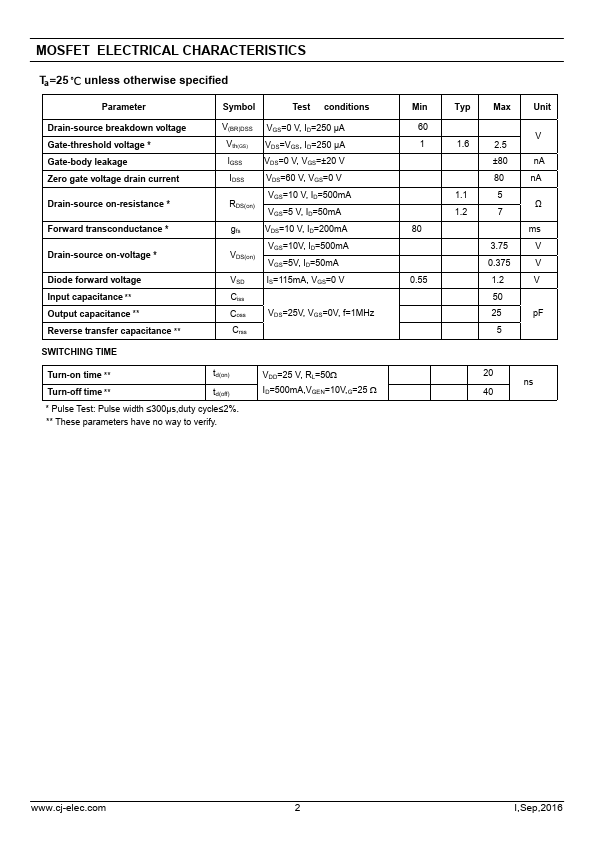
Ta=25 ℃ unless otherwise specified Parameter Symbol Test conditions Drain-source breakdown voltage Gate-threshold voltage * Gate-body leakage Zero gate voltage drain current Drain-source on-resistance * Forward transconductance * Drain-source on-voltage * Diode forward voltage Input capacitance ** Output capacitance ** Reverse transfer capacitance ** V(BR)DSS VGS=0 V, ID=250 µA Vth(GS) VDS=VGS, ID=250 µA lGSS VDS=0 V, VGS=±20 V IDSS VDS=60 V, VGS=0 V RDS(on) VGS=10 V, ID=500mA VGS=5 V, ID=50mA gfs VDS=10 V, ID=200mA VDS(on) VGS=10V, ID=500mA VGS=5V, ID=50mA VSD IS=115mA, VGS=0 V Ciss Coss VDS=25V, VGS=0V, f=1MHz Crss SWITCHING TIME Turn-on time ** td(on) Turn-off time ** td(off) * Pulse Test: Pulse width ≤300µs,duty cycle≤2%. ** These parameters have no way to verify. JCET