JGD MBR0530W
The products shown herein are not designed for use in medical, life-saving, or life-sustaining applications.Customers using or seling these products for use in such applications do so at their own risk and agree to fully indemnify JGD for any damages resulting from such improper use or sale.| Part No. | MBR0530W |
|---|---|
| Datasheet | MBR0530W Download |
| Manufacturer |  JGD |
| Description | Surface Mount Schottky Barrier Diode |
| Buy | Stock & Price |
FEATURES
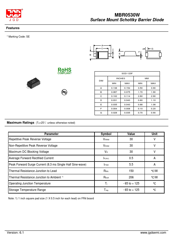
* Marking Code: SE MBR0530W Surface Mount Schottky Barrier Diode A C B DE G FMAXIMUM RATINGS
(TA=25℃ unless otherwise noted) SOD-123F INCHES MM DIM MIN MAX MIN MAX A 0.138 0.154 3.50 3.90 B 0.067 0.075 1.70 1.90 C 0.102 0.114 2.60 2.90 D 0.031 0.043 0.80 1.10 E 0.035 0.043 0.88 1.08 F 0.004 0.008 0.10 0.20 G 0.028 0.035 0.70 0.90 Parameter Repetitive Peak Reverse Voltage Non-Repetitive Peak Reverse Voltage Maximum DC Blocking Voltage Average Forward Rectified Current Peak Forward Surge Current (8.3 ms Single Half Sine-wave) Thermal Resistance Junction to Lead Thermal Resistance Junction to Ambient 1) Operating Junction Temperature Storage Temperature Range Note: 1) 1 inch square pad size (1 X 0.5 inch for each lead) on FR4 board Symbol VRRM VRSM VR IF(AV) IFSM RθJL RθJA Tj Tstg Value 30 30 30 0.5 5.5 150 206 - 65 to + 125 - 65 to + 125 Unit V V V A A ℃/W ℃/W ℃ ℃ Version: 6.1 MBR0530W Surface Mount Schottky Barrier DiodeELECTRICAL CHARACTERISTICS
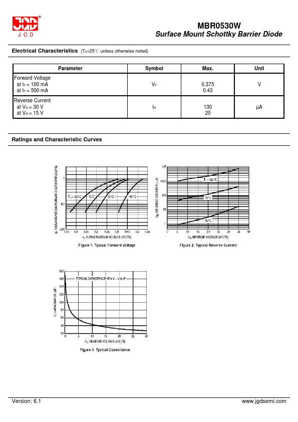
(TA=25℃ unless otherwise noted) Forward Voltage at IF = 100 mA at IF = 500 mA Reverse Current at VR = 30 V at VR = 15 V Parameter Symbol VF IR Max.