JCS90N10 Overview
Key Features
- Low gate charge
- Fast switching
- 100% avalanche tested
- Improved dv/dt capability
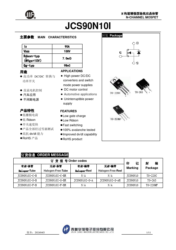
- RoHS product ORDER MESSAGE Order codes
- Derate above Power Dissipa
| Part | JCS90N10 |
|---|---|
| Description | N-CHANNEL MOSFET |
| Category | MOSFET |
| Manufacturer | JILIN SINO |
| Size | 667.91 KB |
| Part Number | Manufacturer | Description |
|---|---|---|
| AP9563GH | Advanced Power Electronics Corp | P-CHANNEL ENHANCEMENT MODE POWER MOSFET |
| FCPF360N65S3R0L | onsemi | N-Channel MOSFET |
| A2SHB | HAOHAI | N-Channel MOSFET |