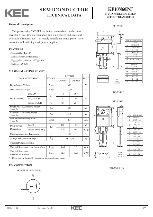
KF10N60P
KF10N60P is N CHANNEL MOS FIELD EFFECT TRANSISTOR manufactured by KEC.
Description
This planar stripe MOSFET has better characteristics, such as fast switching time, low on resistance, low gate charge and excellent avalanche characteristics. It is mainly suitable for active power factor correction and switching mode power supplies. FEATURES
VDSS=600V, ID=10A Drain-Source ON Resistance : RDS(ON)(Max)=0.69 Qg(typ.)= 29.5n C @VGS=10V
KF10N60P/F
N CHANNEL MOS FIELD EFFECT TRANSISTOR
O C F E G B Q I K M L J H P
DIM MILLIMETERS _ 0.2 9.9 + A B C D E F G H I J K L M N
15.95 MAX 1.3+0.1/-0.05 _ 0.1 0.8 + _ 0.2 3.6 + _ 0.1 2.8 + 3.7 0.5+0.1/-0.05 1.5 _ 0.3 13.08 + 1.46 _ 0.1 1.4 + _ 0.1 1.27 + _ 0.2 2.54 + _ 0.2 4.5 + _ 0.2 2.4 + _ 0.2 9.2 +
MAXIMUM RATING (Tc=25
CHARACTERISTIC Drain-Source Voltage Gate-Source Voltage @TC=25 Drain Current @TC=100 Pulsed (Note1) Single Pulsed Avalanche Energy (Note 2) Repetitive Avalanche Energy (Note 1) Peak Diode Recovery dv/dt (Note 3) Drain Power Dissipation Tc=25 Derate above 25
)
RATING SYMBOL KF10N60P VDSS VGSS ID IDP EAS EAR dv/dt PD Tj Tstg 190 1.52 150 -55 150
D NN H
UNIT KF10N60F 600 30 10 6 25 400 16.5 4.5 50 0.4 10- 6- 25- A V V
1 2 3
1. GATE 2. DRAIN 3. SOURCE
TO-220AB
KF10N60F
C m J m J V/ns W W/
MILLIMETERS
Maximum Junction Temperature Storage Temperature Range Thermal Characteristics Thermal Resistance, Junction-to-Case Thermal Resistance, Junction-to-Ambient
Rth JC Rth JA
0.65 62.5
2.5 62.5
/W...