KK4017B
KK4017B is Counter/Divider manufactured by Kodenshi AUK Group.
..
TECHNICAL DATA
Counter/Divider
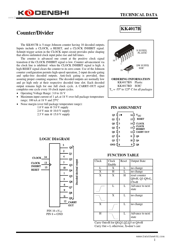
The KK4017B is 5-stage Johnson counter having 10 decoded outputs. Inputs include a CLOCK, a RESET, and a CLOCK INHIBIT signal. Schmitt trigger action in the CLOCK input circuit provides pulse shaping that allows unlimited clock input pulse rise and fall times. The counter is advanced one count at the positive clock signal transition if the CLOCK INHIBIT signal is low. Counter advancement via the clock line is inhibited when the CLOCK INHIBIT signal is high. A high RESET signal clears the counter to its zero count. Use of the Johnson counter configuration permits high-speed operation, 2-input decode-gating and spike-free decoded outputs. Anti-lock gating is provided, thus assuring proper counting sequence. The decoded outputs are normally low and go high only at their respective decoded time slot. Each decoded output remains high for one full clock cycle. A CARRY-OUT signal pletes one cycle every 10 clock input cycles.
- Operating Voltage Range: 3.0 to 18 V
- Maximum input current of 1 µA at 18 V over full package-temperature range; 100 n A at 18 V and 25°C
- Noise margin (over full package temperature range): 1.0 V min @ 5.0 V supply 2.0 V min @ 10.0 V supply 2.5 V min @ 15.0 V supply
N SUFFIX PLASTIC 16 1 16 1 DW SUFFIX SOIC
ORDERING INFORMATION KK4017BN Plastic KK4017BD SOIC TA = -55° to 125° C for all packages
PIN ASSIGNMENT
LOGIC DIAGRAM
FUNCTION TABLE
Clock L X X Clock Enable X H X Reset L L H Output State no change no change reset counter Q0=H, Q1-Q9=L, C0=H Advance to next state no change no change Advance to next state
L X X PIN 16 =VCC PIN 8 = GND H
Carry Out=H for Q0,Q1,Q2,Q3 or Q4=H Carry Out = L otherwise, X=don’t care
..
MAXIMUM RATINGS-
Symbol VCC VIN VOUT IIN PD PD Tstg TL
- Parameter DC Supply Voltage (Referenced to GND) DC Input Voltage (Referenced to GND) DC Output Voltage (Referenced to GND) DC Input Current, per Pin Power Dissipation...