KK74HCT164A
KK74HCT164A is 8-BIT SERIAL-INPUT/PARALLEL-OUTPUT SHIFT RESISTER manufactured by Kodenshi AUK Group.
TECHNICAL DATA
8-BIT SERIAL-INPUT/PARALLEL-OUTPUT SHIFT RESISTER
High-Performance Silicon-Gate CMOS
The KK74HCT164A may be used as a level converter for interfacing TTL or NMOS outputs to high-speed CMOS inputs. The KK74HCT164A is identical in pin out to the LS/ALS164.
- -
- - TTL/NMOS-patible Input Levels. Outputs Directly Interface to CMOS, NMOS and TTL. Operating Voltage Range: 4.5 to 5.5 V Low Input Current: 1.0 µA
ORDERING INFORMATION KK74HCT164AN Plastic KK74HCT164AD SOIC TA = -55° to 125° C for all packages
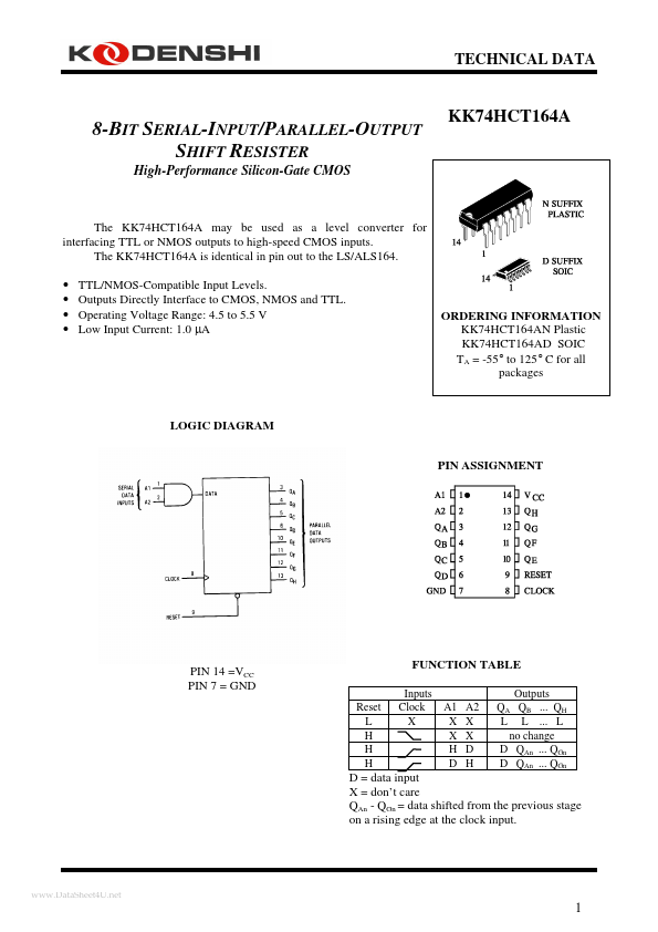
LOGIC DIAGRAM PIN ASSIGNMENT
PIN 14 =VCC PIN 7 = GND
Reset L H H H
FUNCTION TABLE
Inputs Clock X Outputs QA QB ... QH L L ... L no change D QAn ... QGn D QAn ... QGn
A1 X X H D
A2 X X D H
D = data input X = don’t care QAn
- QGn = data shifted from the previous stage on a rising edge at the clock input.
..net
MAXIMUM RATINGS- Parameter Value DC Supply Voltage (Referenced to GND) -0.5 to +7.0 DC Input Voltage (Referenced to GND) -1.5 to VCC +1.5 DC Output Voltage (Referenced to GND) -0.5 to VCC +0.5 DC Input Current, per Pin ±20 DC Output Current, per Pin ±25 DC Supply Current, VCC and GND Pins ±50 Power Dissipation in Still Air, Plastic DIP+ 750 SOIC Package+ 500 Tstg Storage Temperature -65 to +150 TL Lead Temperature, 1 mm from Case for 10 260 Seconds (Plastic DIP or SOIC Package)
- Maximum Ratings are those values beyond which damage to the device may occur. Functional operation should be restricted to the Remended Operating Conditions. +Derating
- Plastic DIP:
- 10 m W/°C from -55° to 125°C SOIC Package: :
- 7 m W/°C from -55° to 125°C Symbol VCC VIN VOUT IIN IOUT ICC PD Unit V V V m A m A m A m W °C °C
REMENDED OPERATING CONDITIONS Symbol VCC VIN, VOUT TA t r, t f Parameter DC Supply Voltage (Referenced to GND) DC Input Voltage, Output Voltage (Referenced to GND) Operating Temperature, All Package Types Input Rise and Fall Time (Figure 1) Min 4.5 0 -55 0 Max 5.5 VCC +125 500 Unit V V °C...