• Part: SMK0990CI
  • Description: Advanced N-Ch Power MOSFET
  • Category: MOSFET
  • Manufacturer: Kodenshi AUK Group
  • Size: 268.81 KB
Download SMK0990CI Datasheet PDF
Kodenshi AUK Group
SMK0990CI
SMK0990CI is Advanced N-Ch Power MOSFET manufactured by Kodenshi AUK Group.
Features - 
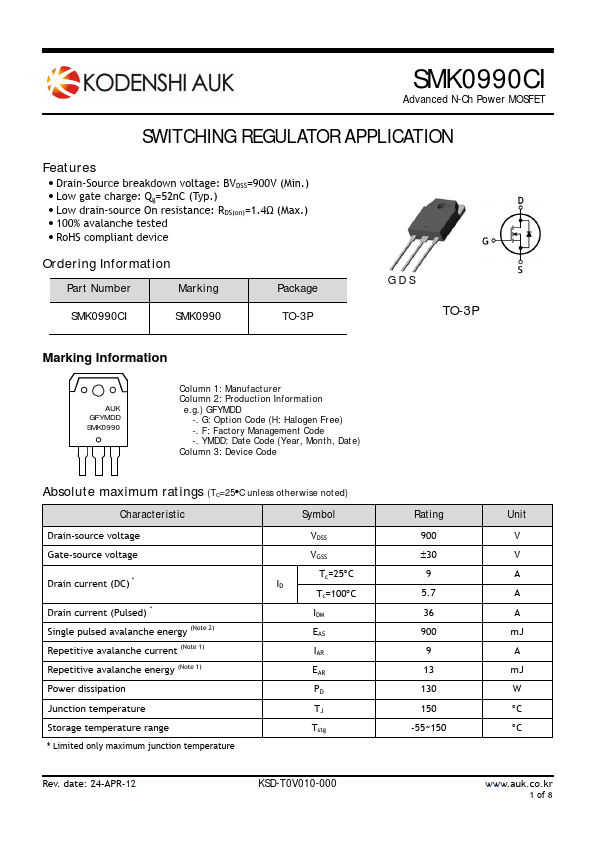
Drain-Source breakdown voltage: BVDSS=900V (Min.) - Low gate charge: Qg=52n C (Typ.) - Low drain-source On resistance: RDS(on)=1.4Ω (Max.) - 100% avalanche tested - Ro HS pliant device Ordering Information Part Number SMK0990CI Marking SMK0990 Package TO-3P GDS TO-3P Marking Information Column 1: Manufacturer Column 2: Production Information e.g.) GFYMDD -. G: Option Code (H: Halogen Free) -. F: Factory Management Code -. YMDD: Date Code (Year, Month, Date) Column 3: Device Code AUK GFYMDD SMK0990 Absolute maximum ratings Characteristic Drain-source voltage Gate-source voltage Drain current (DC) - Drain current (Pulsed) - (TC=25C unless otherwise noted) Symbol VDSS VGSS ID Tc=25C Tc=100C IDM (Note 2) Rating 900 30 9 5.7 36 900 9 13 130 150 -55~150 Unit V V A A A m J A m J W C C Single pulsed avalanche energy Repetitive avalanche current Repetitive avalanche energy Power dissipation Junction temperature Storage temperature range EAS IAR EAR PD TJ Tstg (Note 1) (Note 1) - Limited only maximum junction temperature Rev. date: 24-APR-12 KSD-T0V010-000 .auk.co.kr 1 of 8 Thermal Characteristics Characteristic Thermal resistance, junction to case Thermal resistance, junction to ambient Symbol Rth(j-c) Rth(j-a) Rating Max. 0.96 Max. 40 Unit C/W Electrical Characteristics (TC=25C unless otherwise noted) Characteristic Drain-source breakdown voltage Gate threshold voltage Drain-source cut-off current Gate leakage current Drain-source on-resistance Forward transfer conductance Input capacitance Output capacitance Reverse transfer capacitance Turn-on delay time Rise time (Note 4,5) (Note 4,5) (Note 4,5) (Note 4) Symbol BVDSS VGS(th) IDSS IGSS RDS(ON) gfs Ciss Coss Crss td(on) tr td(off) tf Test Condition ID=250u A, VGS=0 ID=250u A, VDS=VGS VDS=900V, VGS=0V VDS=720V, Tc=125C VDS=0V, VGS=30V VGS=10V, ID=4.5A VDS=10V, ID=4.5A VDS=25V, VGS=0V, f=1.0MHz Min. 900 3 - Typ. 1.12 9.2 2100 175 14 50 120 100 75 52 16 20 Max. 5 1 100 100 1.4...