2SJ325
2SJ325 is MOS Field Effect Power Transistors manufactured by Kexin Semiconductor.
Features
Low on-state resistance RDS(on)=83m (VGS=-10V,ID=-2A) RDS(on)=0.15 (VGS=-4V,ID=-1.6A) Built-in G-S Gate Protection Diode
+0.2 9.70 -0.2
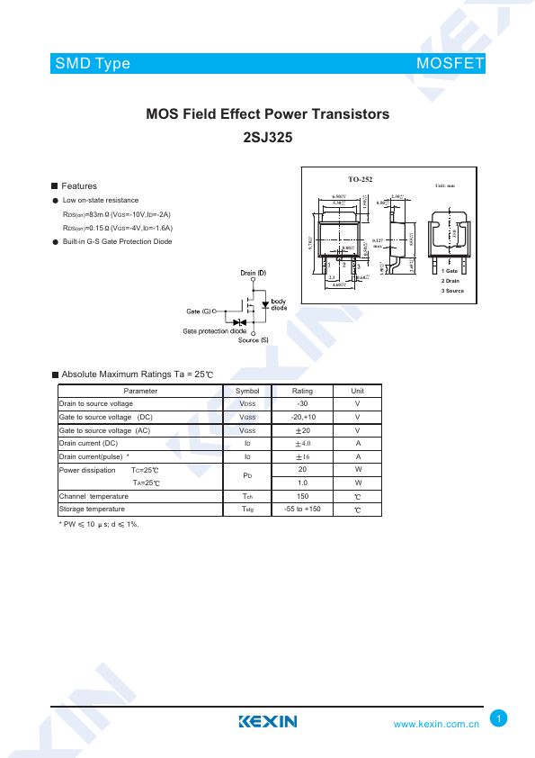
TO-252
6.50+0.15 -0.15
5.30+0.2 -0.2
2.30+0.1 -0.1
0.50+0.8 -0.7
Unit: mm
+0.15 1.50 -0.15
+0.15 5.55 -0.15
0.80+0.1 -0.1
0.127 max
2.3 4.60+0.15
-0.15
0.60+0.1 -0.1
+0.15 0.50 -0.15
+0.28 1.50 -0.1
+0.25 2.65 -0.1
1 Gate 2 Drain 3 Source
Absolute Maximum Ratings Ta = 25
Parameter Drain to source voltage Gate to source voltage (DC) Gate to source voltage (AC) Drain current (DC) Drain current(pulse)
- Power dissipation TC=25
TA=25 Channel temperature Storage temperature
Symbol
Rating
Unit
VDSS
-30
VGSS
-20,+10
VGSS
Tch...