Datasheet4U Logo Datasheet4U.com

2SJ605 - MOS Field Effect Transistors

Key Features

  • Super low on-state resistance: RDS(on)1 = 20 m RDS(on)2 = 31 m MAX. (VGS = -10 V, ID = -33 A) + 0 .2 8 .7 -0 .2 MAX. (VGS = -4.0 V, ID = -33 A) Low input capacitance Ciss = 4600 pF TYP. (VDS = -10 V, VGS = 0 A) +0.1 1.27-0.1 0.1max +0.1 0.81-0.1 2.54 +0.2 -0.2 +0.1 5.08-0.1 + 0 .2 2 .5 4 -0 .2 Built-in gate protection diode + 0 .2 5 .2 8 -0 .2 + 0 .2 1 5 .2 5 -0 .2 2.54 +0.2 0.4-0.2 Absolute Maximum Ratings Ta = 25 Parameter Drain to Source Voltage Gate to Source Voltage Drain Curre.

📥 Download Datasheet

Full PDF Text Transcription (Reference)

The following content is an automatically extracted verbatim text from the original manufacturer datasheet and is provided for reference purposes only.

View original datasheet text
SMD Type 
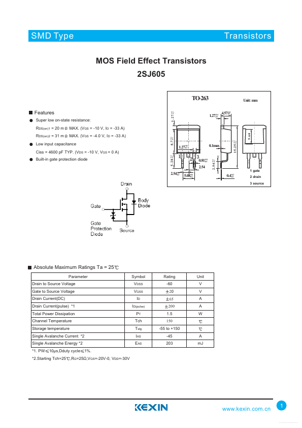
MOS Field Effect Transistors 2SJ605 TO-263 + 0 .1 1 .2 7 -0 .1 Transistors IC Unit: mm +0.1 1.27-0.1 +0.2 4.57-0.2 Features Super low on-state resistance: RDS(on)1 = 20 m RDS(on)2 = 31 m MAX. (VGS = -10 V, ID = -33 A) + 0 .2 8 .7 -0 .2 MAX. (VGS = -4.0 V, ID = -33 A) Low input capacitance Ciss = 4600 pF TYP. (VDS = -10 V, VGS = 0 A) +0.1 1.27-0.1 0.1max +0.1 0.81-0.1 2.54 +0.2 -0.2 +0.1 5.08-0.1 + 0 .2 2 .5 4 -0 .2 Built-in gate protection diode + 0 .2 5 .2 8 -0 .2 + 0 .2 1 5 .2 5 -0 .2 2.54 +0.2 0.4-0.2 Absolute Maximum Ratings Ta = 25 Parameter Drain to Source Voltage Gate to Source Voltage Drain Current(DC) Drain Current(pulse) *1 Total Power Dissipation Channel Temperature Storage temperature Single Avalanche Current *2 Single Avalanche Energy *2 *1.