Datasheet4U Logo Datasheet4U.com

2SJ605 - MOS FIELD EFFECT TRANSISTOR

General Description

The 2SJ605 is P-channel MOS Field Effect Transistor designed for high current switching applications.

Key Features

  • Super low on-state resistance: RDS(on)1 = 20 mΩ MAX. (VGS =.
  • 10 V, ID =.
  • 33 A) RDS(on)2 = 31 mΩ MAX. (VGS =.
  • 4.0 V, ID =.
  • 33 A).
  • Low input capacitance ! Ciss = 4600 pF TYP. (VDS =.
  • 10 V, VGS = 0 A).
  • Built-in gate protection diode Note TO-220SMD package is produced only in Japan. (TO-220AB).

📥 Download Datasheet

Full PDF Text Transcription (Reference)

The following content is an automatically extracted verbatim text from the original manufacturer datasheet and is provided for reference purposes only.

View original datasheet text
DATA SHEET MOS FIELD EFFECT TRANSISTOR 2SJ605 SWITCHING P-CHANNEL POWER MOS FET INDUSTRIAL USE DESCRIPTION The 2SJ605 is P-channel MOS Field Effect Transistor designed for high current switching applications. 
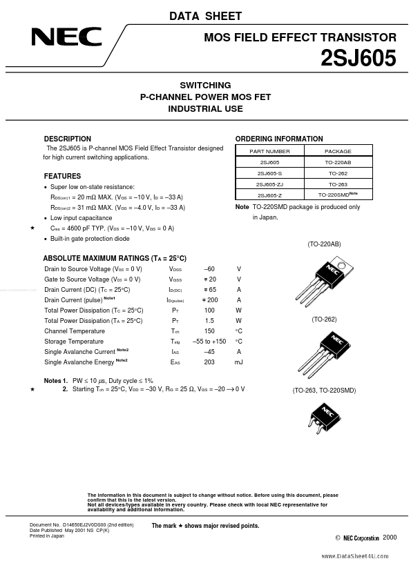
ORDERING INFORMATION PART NUMBER 2SJ605 2SJ605-S 2SJ605-ZJ 2SJ605-Z PACKAGE TO-220AB TO-262 TO-263 TO-220SMDNote FEATURES • Super low on-state resistance: RDS(on)1 = 20 mΩ MAX. (VGS = –10 V, ID = –33 A) RDS(on)2 = 31 mΩ MAX. (VGS = –4.0 V, ID = –33 A) • Low input capacitance ! Ciss = 4600 pF TYP. (VDS = –10 V, VGS = 0 A) • Built-in gate protection diode Note TO-220SMD package is produced only in Japan. (TO-220AB) ABSOLUTE MAXIMUM RATINGS (TA = 25°C) Drain to Source Voltage (VGS = 0 V) Gate to Source Voltage (VDS = 0 V) www.DataSheet4U.