Kexin Electronics FDB2670
N-Channel MOSFET
| Part No. | FDB2670 |
|---|---|
| Datasheet | FDB2670 Download |
| Manufacturer | Kexin Electronics |
| Description | N-Channel MOSFET |
| Buy | Stock & Price |
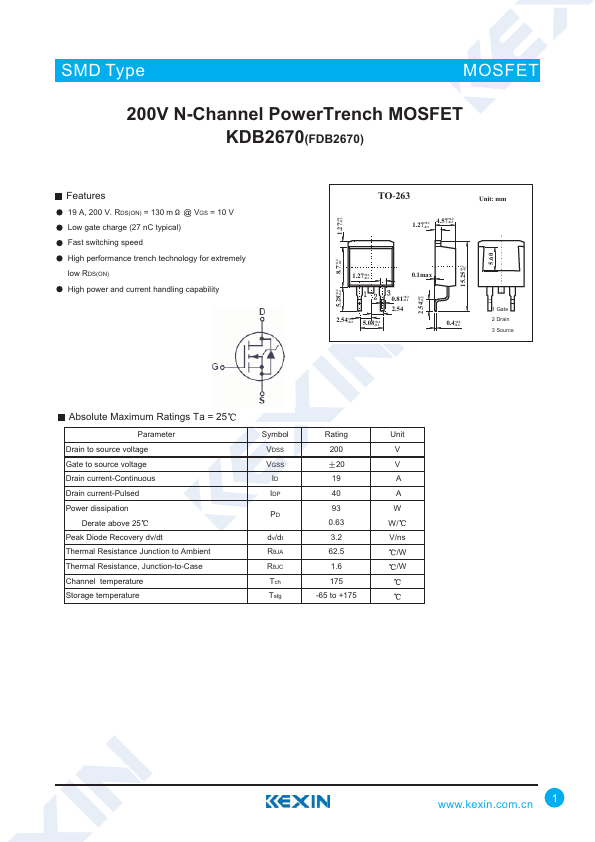
FEATURES
19 A, 200 V. RDS(ON) = 130 m @ VGS = 10 V Low gate charge (27 nC typical) Fast switching speed High performance trench technology for extremely low RDS(ON) High power and current handling capability +0.25.28 -0.2 +0.28.7 -0.2 TO-263 +0.2 4.57+0.1 -0.2 1.27-0.1 Unit: mm +0.11.27 -0.1 +0.22.54 -0.2 15.25-+00..22 5.60 1.27+0.1 -0.1 0.1max 2.54+0.2 -0.2 5.08+0.1 -0.1 0.81+0.1 -0.1 2.54 0.4+0.2 -0.2 1 Gate 2 Drain 3 SourceABSOLUTE MAXIMUM RATINGS
Ta = 25 Parameter Drain to source voltage Gate to source voltage Drain current-Continuous Drain current-Pulsed Power dissipation Derate above 25 Peak Diode Recovery dv/dt Thermal Resistance Junction to Ambient Thermal Resistance, Junction-to-Case Channel temperature Storage temperature Symbol VDSS VGSS ID IDP PD dv/dt RèJA RèJC Tch Tstg Rating 200 20 19 40 93 0.63 3.2 62.5 1.6 175 -65 to +175 Unit V V A A W W/ V/ns /W /W 1 SMD Type MOSFET KDB2670(FDB2670)ELECTRICAL CHARACTERISTICS
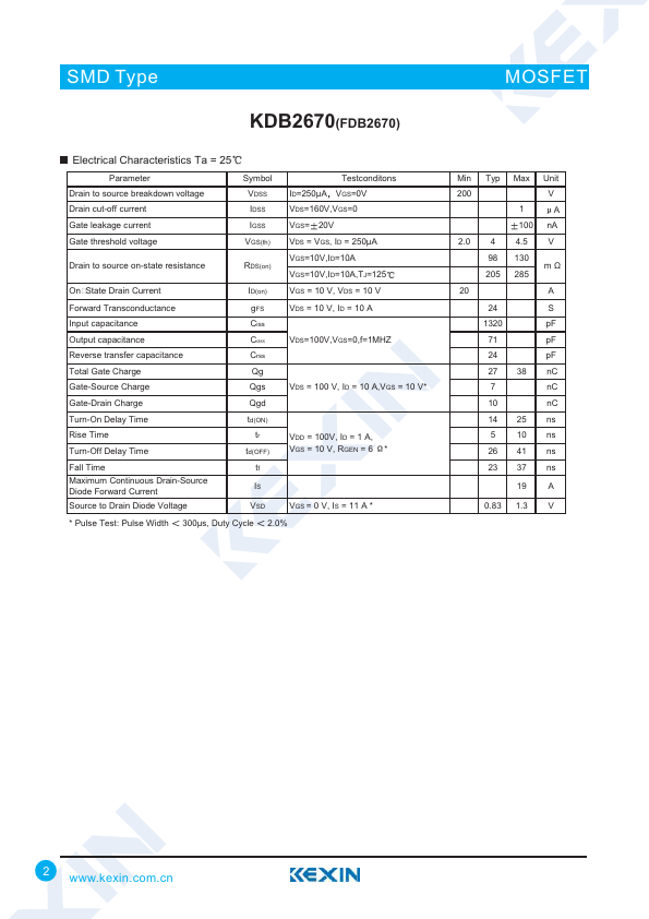
Ta = 25 Parameter Drain to source breakdown voltage Drain...