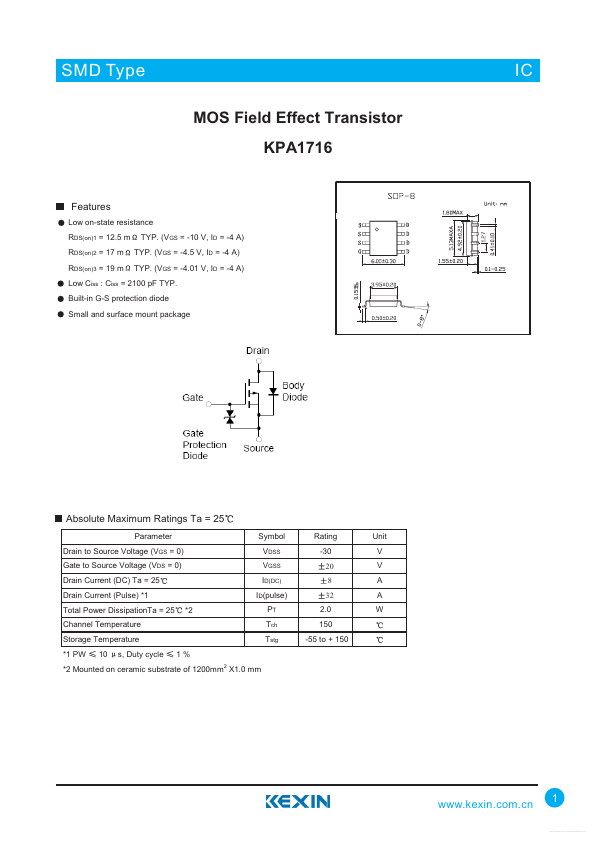
Datasheet4U Logo Datasheet4U.com

KPA1716 - MOS Field Effect Transistor

Key Features

  • Low on-state resistance RDS(on)1 = 12.5 m RDS(on)2 = 17 m RDS(on)3 = 19 m TYP. (VGS = -10 V, ID = -4 A) TYP. (VGS = -4.5 V, ID = -4 A) TYP. (VGS = -4.01 V, ID = -4 A) Low Ciss : Ciss = 2100 pF TYP. Built-in G-S protection diode Small and surface mount package Absolute Maximum Ratings Ta = 25 Parameter Drain to Source Voltage (VGS = 0) Gate to Source Voltage (VDS = 0) Drain Current (DC) Ta = 25 Drain Current (Pulse).
  • 1 Total Power DissipationTa = 25 Channel Temperature Storage Temperature.

📥 Download Datasheet

Full PDF Text Transcription (Reference)

The following content is an automatically extracted verbatim text from the original manufacturer datasheet and is provided for reference purposes only.

View original datasheet text
SMD Type MOS Field Effect Transistor KPA1716 IC IC Features Low on-state resistance RDS(on)1 = 12.5 m RDS(on)2 = 17 m RDS(on)3 = 19 m TYP. (VGS = -10 V, ID = -4 A) TYP. (VGS = -4.5 V, ID = -4 A) TYP. (VGS = -4.01 V, ID = -4 A) Low Ciss : Ciss = 2100 pF TYP. Built-in G-S protection diode Small and surface mount package Absolute Maximum Ratings Ta = 25 Parameter Drain to Source Voltage (VGS = 0) Gate to Source Voltage (VDS = 0) Drain Current (DC) Ta = 25 Drain Current (Pulse) *1 Total Power DissipationTa = 25 Channel Temperature Storage Temperature *1 PW 10 s, Duty cycle 1% *2 Symbol VDSS VGSS ID(DC) ID(pulse) PT Tch Tstg Rating -30 20 8 32 2.0 150 -55 to + 150 Unit V V A A W *2 Mounted on ceramic substrate of 1200mm2 X1.0 mm www.kexin.com.cn 1 Free Datasheet http://www.datasheet4u.