Datasheet Summary
SMD Type
MOS Field Effect Transistor KPA1758
IC IC
Features
Dual MOS FET chips in small package 2.5 V gate drive type low on-state resistance RDS(on)1 = 30 m RDS(on)2 = 40 m (MAX.) (VGS = 4.5 V, ID = 3.0 A) (MAX.) (VGS = 2.5 V, ID = 3.0 A)
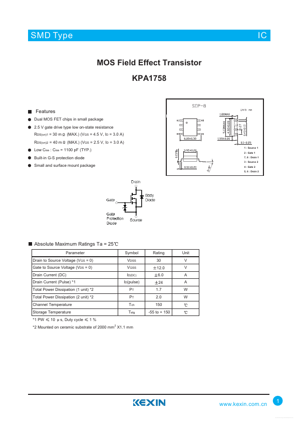
1 : Source 1 2 : Gate 1 7, 8 : Drain 1 3 : Source 2 4 : Gate 2 5, 6 : Drain 2
Low Ciss : Ciss = 1100 pF (TYP.) Built-in G-S protection diode Small and surface mount...