KVN4525E6
KVN4525E6 is 250V N-Channel Enhancement Mode MOSFET manufactured by Kexin Semiconductor.
Features
High voltage Low on-resistance Fast switching speed Low gate drive Low threshold
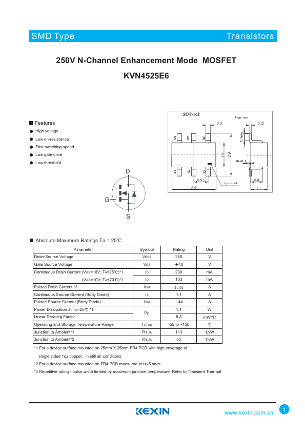
Unit: mm 1 pin mark
Absolute Maximum Ratings Ta = 25
Parameter Drain-Source Voltage Gate Source Voltage Continuous Drain Current (VGS=10V; TA=25 )- 1
(VGS=10V; TA=70 )- 1 Pulsed Drain Current
- 3 Continuous Source Current (Body Diode) Pulsed Source Current (Body Diode) Power Dissipation at TA=25
- 1 Linear Derating Factor Operating and Storage Temperature Range Junction to Ambient- 1 Junction to Ambient- 2
Symbol VDSS VGS ID ID IDM IS ISM
Tj:Tstg R JA R JA
Rating 250 40 230 183
1.1 1.44 1.1 8.8 -55 to +150 113 65
Unit V V m A m A A A A W m W/
/W /W
- 1 For a device surface mounted on 25mm X 25mm FR4 PCB with high coverage of single sided 1oz copper, in still air conditions
- 2 For a device surface mounted on FR4 PCB measured at t 5 secs.
- 3 Repetitive rating
- pulse width limited by maximum junction temperature. Refer to Transient Thermal
.kexin..cn 1
SMD Type
Transist Io Crs
Electrical Characteristics Ta = 25
Parameter
Symbol
Testconditons
Drain-Source Breakdown Voltage
V(BR)DSS ID=1m A, VGS=0V
Zero Gate Voltage Drain Current
IDSS
VDS=250V, VGS=0V
Gate-Body Leakage
IGSS
VGS= 40V, VDS=0V
Gate-Source Threshold Voltage
VGS(th) ID=1m A, VDS= VGS
VGS=10V, ID=500m A
Static Drain-Source On-State Resistance
- 1 RDS(on) VGS=4.5V, ID=360m A
VGS=2.4V, ID=20m...