NDS352AP Overview
Key Features
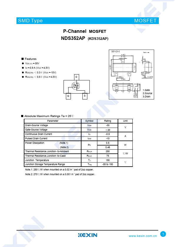
- VDS (V) =-30V
- ID =-0.9 A (VGS =-4.5V)
- RDS(ON) < 0.3Ω (VGS =-10V)
| Part | NDS352AP |
|---|---|
| Description | P-Channel MOSFET |
| Category | MOSFET |
| Manufacturer | Kexin Semiconductor |
| Size | 1.49 MB |
| Part Number | Manufacturer | Description |
|---|---|---|
| NDS352AP | Fairchild Semiconductor | P-Channel Logic Level Enhancement Mode Field Effect Transistor |
| 512-NDS352AP | Fairchild Semiconductor | Low Power MOSFET |
| NDS352P | Fairchild Semiconductor | P-Channel Logic Level Enhancement Mode Field Effect Transistor |
| NDS355AN | Fairchild Semiconductor | N-Channel Logic Level Enhancement Mode Field Effect Transistor |
| NDS351N | Fairchild Semiconductor | N-Channel Logic Level Enhancement Mode Field Effect Transistor |